

Analyzing global electronics design architectures and how foundational board layers drive modern device reliability, scalability, and cost efficiency.
Utilizing high-grade FR4 (Tg130 to Tg170), CEM-3, and metal-core substrates (MCPCBs) ensures optimal mechanical strength and structural consistency. These raw materials prevent delamination during high-temperature reflow soldering processes, safeguarding circuit traces from early degradation.
For high-volume production, Single-Sided PCBs deliver an unmatched cost-to-performance ratio. Industries requiring straightforward circuit routes—such as LED systems, power supplies, and sensor relays—benefit from reduced prototyping costs and rapid fabrication cycles without sacrificial reliability.
Double-Sided PCBs utilize advanced copper electroplating to deposit conductive layers inside drilled vias. This technique establishes reliable connections between top and bottom layers, enabling tighter routing paths, higher components densities, and improved signal paths.
Understanding physical dimensions, material grades, surface finishes, and manufacturing tolerances to guide your procurement choices.
| Technical Metric / Capability | Single-Sided PCBs | Double-Sided PCBs (Plated & Non-Plated) |
|---|---|---|
| Base Substrate Materials | FR-4, FR-1, CEM-1, CEM-3, Aluminum Core (MCPCB) | FR-4 Standard/High-Tg, Polyimide (Flexible), Taconic High-Frequency |
| Dielectric Thickness Range | 0.2mm to 3.2mm (Typical: 1.6mm) | 0.4mm to 4.0mm (Custom thin options available) |
| Copper Foil Weight (Finished) | 0.5 oz, 1.0 oz, 2.0 oz, up to 3.0 oz (Heavy Copper) | 0.5 oz, 1.0 oz, 2.0 oz, up to 6.0 oz (Heavy copper applications) |
| Minimum Trace Width / Space | 0.15mm (6 mil) / 0.15mm (6 mil) | 0.10mm (4 mil) / 0.10mm (4 mil) |
| Hole Size (Min. Finished) | 0.50mm via mechanical drilling | 0.20mm via mechanical drilling; 0.10mm via laser drilling |
| Surface Finish Chemistry | Lead-free HASL, OSP, Immersion Gold (ENIG) | ENIG, HASL, Immersion Silver, Hard Gold Plating, OSP |
| Thermal Conductivity (Metal Base) | 1.0 W/m-K to 4.0 W/m-K (For LED / Power applications) | Up to 3.0 W/m-K with thermal via array structures |
| Solder Mask Colors Available | Green, White, Matte Black, Blue, Red, Yellow | Green, Blue, Black, White (High-reflectivity LED Grade), Red |
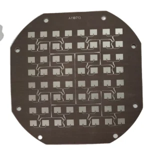
Industrial electronics demand specialized board architectures to balance durability and cost. Single-sided metal-core PCBs are dominating the green lighting sector, providing low-thermal resistance paths crucial for high-power LED matrices.
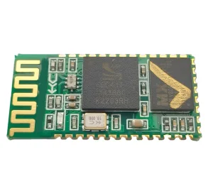
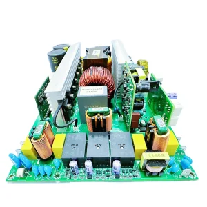
Concurrently, double-sided PCBs act as the cornerstone for smart meters, power distribution units, consumer peripherals, and IoT modules. By leveraging plated through-holes (PTH), developers route signal and ground systems across opposing layers, controlling electromagnetic interference (EMI) while minimizing overall footprints.
Our global supply lines cater to OEMs, EMS firms, and industrial designers who demand trace integrity, short fabrication lead times, and predictable electrical parameters under variable environmental conditions.

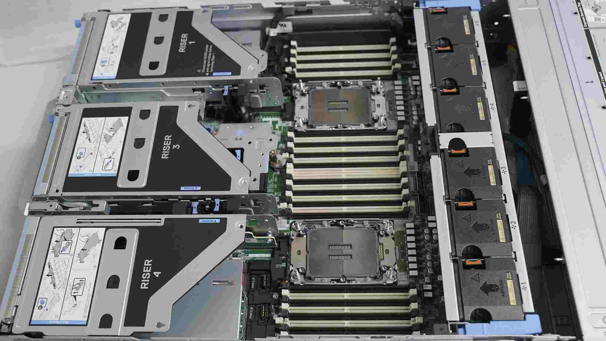
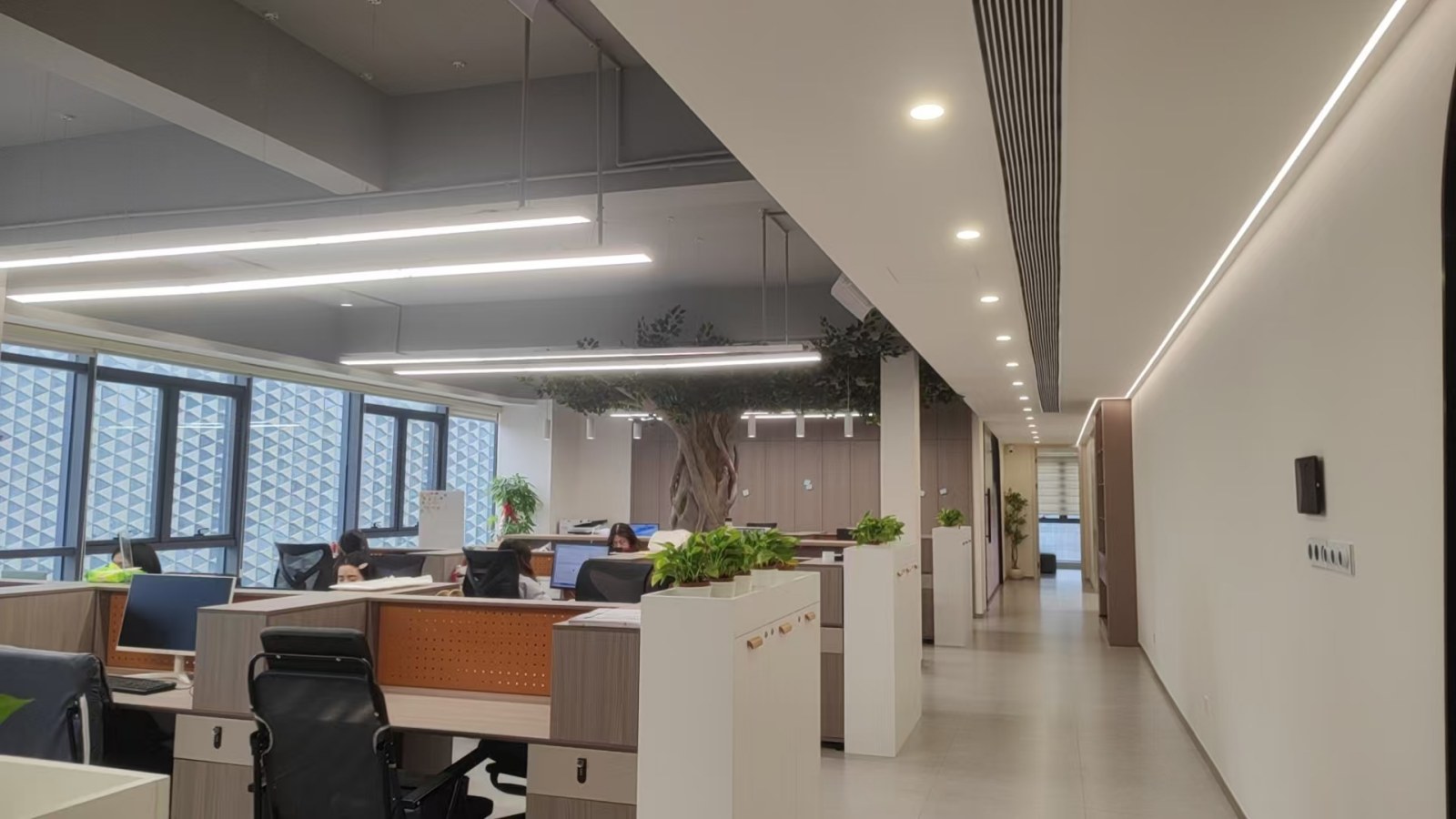
A professional DDR5 memory and high-performance PCB assembly (PCBA) manufacturer based in Shenzhen, China, servicing advanced global engineering markets.
Velmix Technology Co., Ltd. is a professional DRAM and PCB assembly manufacturer based in Shenzhen, China, specializing in the research, development, production, and global distribution of high-reliability memory modules and multi-layer, double-sided, and single-sided printed circuit board systems. Since its establishment in 2017, Velmix has focused on delivering robust and high-speed electrical solutions for consumer electronics, industrial automation, server farms, smart grid applications, and edge devices.
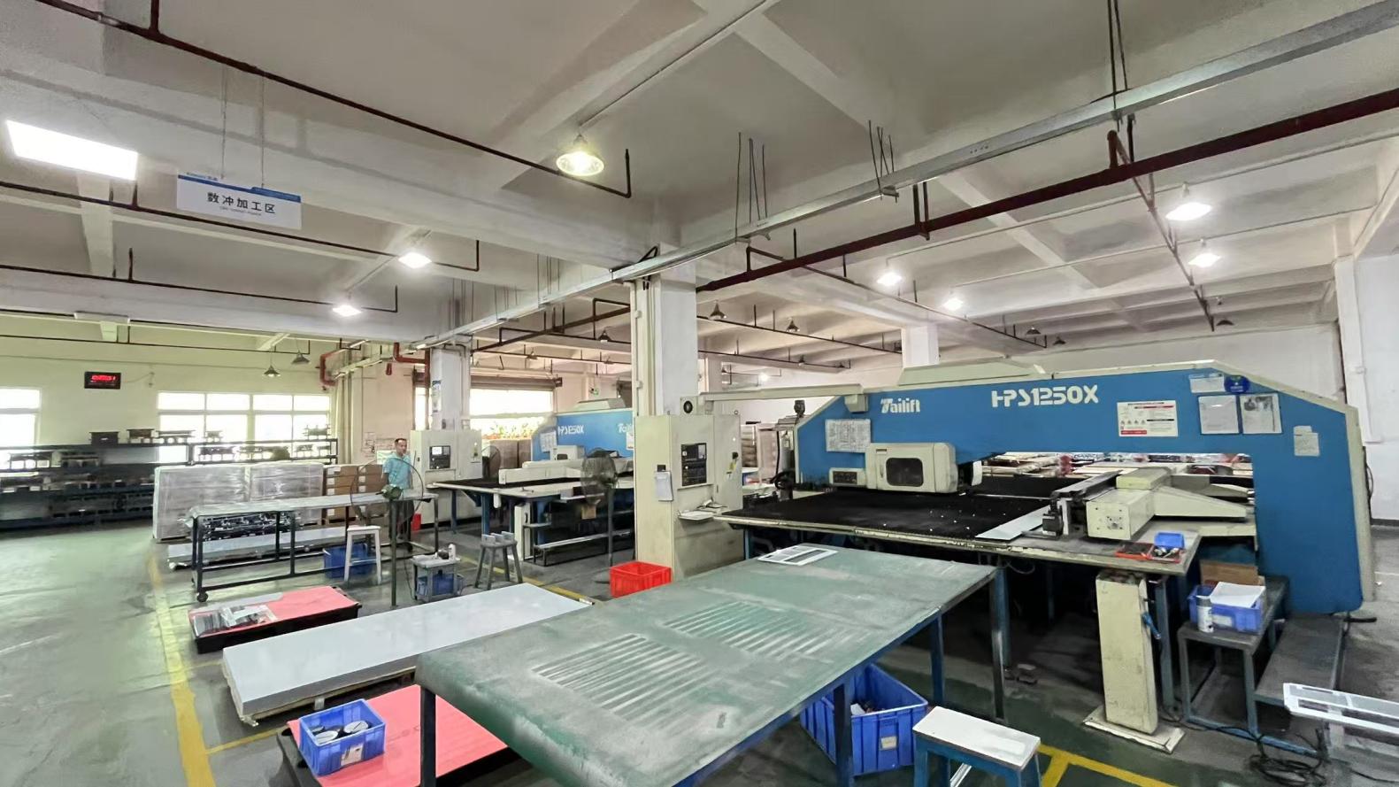
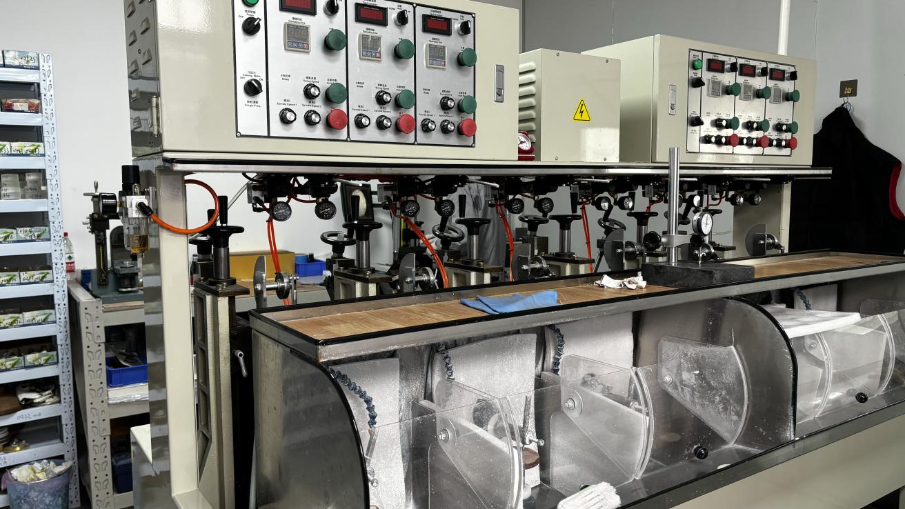
Operating from a modern, precision-optimized facility covering 368㎡, we consolidate automated SMT assembly lines, cleanrooms, and testing blocks under one roof. Our experienced engineering division continuously innovates to deliver PCB solutions optimized for high-speed signal pathways, advanced thermal management, and low noise thresholds.
Velmix serves dynamic markets across 40 countries, providing flexible OEM and ODM manufacturing services for global technology brands, system integrators, distributors, and device manufacturers. By focusing on product consistency, rapid delivery schedules, and thorough electrical certification, we have built long-term partnerships across North America, Europe, Southeast Asia, and the Middle East.
| Comprehensive Company Parameters & Operations Details | |
|---|---|
| Company Name | Velmix Technology Co., Ltd. |
| Established | 2017 |
| Facility Area | 368㎡ |
| Annual Export Revenue | USD 18.6 Million |
| Export Experience | 8 Years |
| Industry Experience | 15 Years |
| Quality Control | 100% Full Inspection Before Shipment |
| Product Inspection Methods | Signal Integrity Test, Burn-in Test, Compatibility Test, Functional Test & Random Sampling |
| QC Staff | 56 Employees |
| Business Type | Manufacturer & Exporter |
| Main Markets | North America, Europe, Southeast Asia, Middle East & South America |
| Supply Chain Partners | 986+ |
| Main Customer Types | Brand Owners, OEM Manufacturers, System Integrators, Distributors & Wholesalers |
| R&D Capability | Independent Product Design, PCB Development & Firmware Optimization |
| Customization Options | OEM, ODM, Private Label, Customized Capacity, Heat Spreader, PCB Color & Packaging |
| New Products Launched Last Year | 138 Models |
| R&D Engineers | 84 Engineers |
Understanding environmental trends, micro-vias, heat dissipation, and material advances shaping the next generation of boards.
Global environmental mandates are driving the transition to halogen-free materials and lead-free HASL/ENIG surface treatments. We design PCBs that meet strict EU RoHS and REACH requirements while keeping solderability and thermal stress tolerances high.
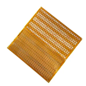
Modern devices require highly integrated layouts. By utilizing ultra-thin single/double-sided flexible circuits (FPCs) made of high-grade polyimides, we allow developers to fit complex components into tight envelopes, reducing weight and eliminating connectors.
To eliminate manual verification errors, our factory deploys automated optical inspection (AOI) systems powered by predictive defect algorithms. This tech catches micro-fissures, solder bridging, and misalignments before shipping, guaranteeing high yields.
How we ensure electrical and mechanical reliability across our single-sided and double-sided boards for international markets.
Every single-sided and double-sided board undergoes strict functional tests. We use automatic flying probe testing (FPT) for quick prototypes and dedicated fixture testing (bed-of-nails) for high-volume orders. These checks confirm trace continuity and isolation resistance, eliminating open or short circuits.
In addition, thermal shock and burn-in tests evaluate how components perform under extreme shifts in temperature, preventing field failures in automotive and outdoor environments.
Our manufacturing and assembly processes strictly follow the IPC-A-600 standard (Class 2 and Class 3 targets). This ensures proper registration, consistent plating depth, and minimal solder mask offsets. We source materials certified under UL 94V-0 for flammability resistance to ensure peace of mind.
With an experienced logistics setup and 8 years of export history, we manage clearance paperwork for North American, European, and Asian ports, offering DAP/DDP options to streamline your supply chain.
Clear, direct, and technically accurate answers to help guide your single-sided and double-sided PCB orders.
A single-sided PCB has a conductive copper layer on only one side of the dielectric substrate, making it perfect for simple, cost-sensitive designs. A double-sided PCB has copper layers on both sides, allowing for traces to cross paths via plated through-holes (PTH). This design supports more complex circuits and higher component density.
For general-purpose designs, Lead-Free HASL is cost-effective and easy to solder. For fine-pitch components (like BGAs or small QFNs) and long shelf life, we recommend Immersion Gold (ENIG). It provides a flat landing pad, excellent oxidation resistance, and is fully RoHS compliant.
Metal-core PCBs, typically using an aluminum base, quickly transfer heat away from hot active components (like high-power LEDs or power transistors) through a thin, thermally conductive dielectric layer. This offers much better heat dissipation than standard FR4, keeping operating temperatures low and extending device lifespan.
We perform 100% inspections. Every production batch undergoes automated optical inspection (AOI) to catch trace defects and solder bridging. We verify electrical continuity using flying probe testing (FPT) or custom test fixtures, and we use X-ray analysis to inspect plating quality inside the through-holes.
Yes. While standard green is the most common option, we offer a range of colors including white (excellent for LED backlights due to its high reflectivity), matte black, glossy black, blue, red, and yellow.
Quick-turn prototypes for single or double-sided PCBs can be produced in 24 to 48 hours. Standard production orders typically ship within 7 to 10 working days, depending on order size, layout complexity, and the chosen surface finish.
 Velmix