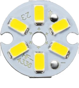
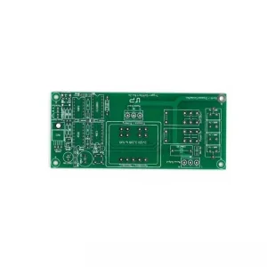
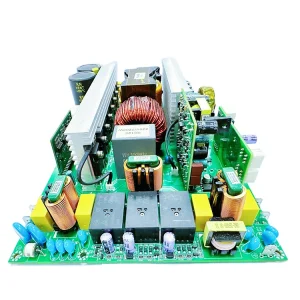
As solid-state lighting technology advances towards higher lumens-per-watt ratios, the core technical bottleneck remains thermal dissipation. High-power LED chips emit significant heat focused at minute junction points. Without efficient heat dissipation, junction temperatures spike, resulting in severe lux degradation, color-shifting, and premature driver or chip failure.
This is where specialized LED PCBs (Metal Core Printed Circuit Boards, or MCPCBs) become critical. Unlike standard FR4 substrates, which exhibit low thermal conductivity (~0.25 W/m·K), modern LED PCBs utilize metallic cores—primarily aluminum or copper—fused with thin, highly-conductive dielectric layers. This allows the system to achieve thermal conductivity values ranging from 1.0 W/m·K to over 8.0 W/m·K, directly preserving component lifespans and ensuring system reliability.
As a leading exporter and manufacturer, our manufacturing frameworks prioritize heat management, mechanical stability, and copper thickness control, translating directly to cost savings and failure rate reductions for international OEMs.
Industrial procurement teams look beyond unit prices. Real value lies in the optimization of the thermal interface material (TIM), precise dielectric layer insulation resistance, and the solderability of SMD light-emitting beads. Standardizing these processes is essential to mitigate field failures in challenging outdoor environments like municipal roadways, high-bay warehouses, and automotive headlight modules.
The industrial concentration in Shenzhen, Guangdong offers unmatched efficiency, component sourcing depth, and logistical speed. Here is how our localized supply chain translates into bottom-line advantages for international buyers.
China is home to the world's most concentrated ecosystem for copper-clad laminates (CCL), high-grade aluminum substrates, and high-performance dielectric resins. This proximity minimizes raw material lead times and insulates international clients from localized supply chain disruptions.
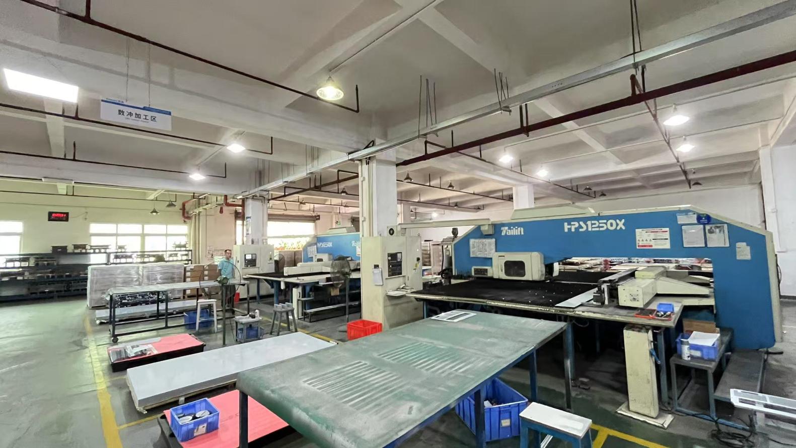
Our production facilities utilize modern machinery, including high-speed Yamaha and Panasonic SMT lines, automated optical inspection (AOI), and continuous vacuum lamination systems. This high degree of automation maintains stable yields for high-volume orders.
Speed to market is critical. Our Shenzhen-based engineering team provides quick turnaround design validation, Design for Manufacturing (DFM) reviews, and rapid prototype fabrication, allowing customers to transition smoothly from proof-of-concept to volume manufacturing.
Understanding substrate limitations is key to successful system design. Below is a comparative guide showing the differences between traditional FR4 boards and metal core boards for light-emitting designs.
| Performance Characteristic | Standard FR4 Substrate | Aluminum Base MCPCB | Copper Base MCPCB | Direct Copper Bond (DCB) Ceramic |
|---|---|---|---|---|
| Thermal Conductivity | 0.20 - 0.25 W/m·K | 1.0 - 3.0 W/m·K | 4.0 - 8.0 W/m·K | 24 - 180 W/m·K |
| Coefficient of Thermal Expansion (CTE) | 14 - 18 ppm/C (X/Y axis) | 22 ppm/C (Matches Al housing) | 17 ppm/C (Matches Copper) | 5 - 7 ppm/C (Best matches Silicon) |
| Dielectric Strength (kV/mm) | 20 - 30 | 3 - 8 (Controlled layer thickness) | 3 - 8 | >15 (Inherent dielectric property) |
| Mechanical Rigidity | Moderate (requires housing support) | High (integrates as structural element) | Very High | Brittle (susceptible to shock) |
| Primary Target Application | Low-power displays, indicator lights | Commercial fixtures, streetlights | Automotive LED heads, spotlights | Concentrated solar, aerospace, high-power arrays |
| Cost Profile | Low (baseline standard) | Moderate (optimal cost-performance) | Premium | High Specialization |
Note: Operating high-power LED systems with junction temperatures exceeding 85°C can cause degradation in lumen output. We advise using Aluminum MCPCBs at minimum for any fixture operating above 5W.
From deep-sea searchlights to safety-critical automotive lighting, our products are engineered for specific, high-demand operating conditions.
Modern vehicles demand high reliability. Our automotive-grade LED PCBs utilize 1.6mm thin-profile aluminum core laminates paired with high-performance copper traces. These systems are qualified to withstand ongoing vibration, thermal shock profiles ranging from -40°C to 125°C, and damp-heat cycles, supporting applications from adaptive high beams (ADB) to interior dashboard modules.
Horticulture lighting requires high continuous wattage and exposure to moisture and fertilizers. Our MCPCBs feature specialized white solder masks resistant to UV yellowing and moisture-barrier coatings, ensuring consistent light spectrum output and avoiding corrosion in grow houses.
Outdoor municipal lighting demands lifespans exceeding 50,000 hours. Our designs feature robust surge protection layouts, heavy copper plating, and high-dielectric breakdown thermal layers (up to 6kV isolation) to protect sensitive drive electronics from lightning strikes and grid transients.
For chemical and heavy manufacturing environments, we manufacture LED PCBs designed to operate at elevated temperatures. By bonding aluminum cores directly to heavy-duty heat sinks, we eliminate structural hotspots, ensuring compliance with hazardous location (Explosion-Proof Class I Div 2) temperature ratings.
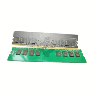
Established in 2017, Velmix Technology Co., Ltd. is an electronics manufacturer based in Shenzhen, China. While specialized in manufacturing high-performance DRAM memory solutions and high-density PCB designs, our operations include state-of-the-art SMT placement, high-density interconnections (HDI), and thermal substrate integrations.
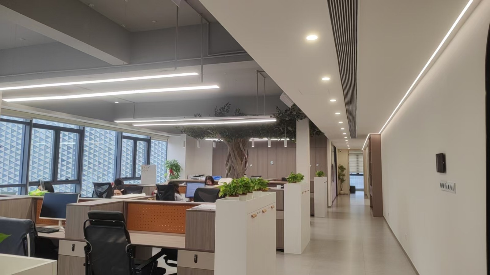
Operating from a modern facility in Shenzhen's electronics manufacturing zone, we provide OEM/ODM production services to partners in over 40 countries. With 15 years of industry experience, Velmix delivers high product reliability through strict supply chain management and standardized testing protocols.
Our engineering division supports global clients through design layout validation, component sourcing, and assembly optimization. Our commitment to strict quality control ensures that our printed circuit assemblies and memory modules meet international standards for performance and reliability.
| Key Organizational Parameters | |
|---|---|
| Company Name | Velmix Technology Co., Ltd. |
| Established | 2017 |
| Facility Area | 368㎡ |
| Annual Export Revenue | USD 18.6 Million |
| Export Experience | 8 Years |
| Industry Experience | 15 Years |
| Quality Control | 100% Full Inspection Before Shipment |
| QC Staff | 56 Employees |
| Business Type | Manufacturer & Exporter |
| Main Markets | North America, Europe, Southeast Asia, Middle East & South America |
| R&D Capability | Independent Design, PCB Development & Firmware Optimization |
| R&D Engineers | 84 Engineers |
We maintain modern assembly lines, optical scanners, and testing laboratories to ensure consistent quality for all shipped items.

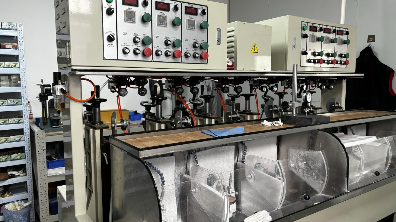
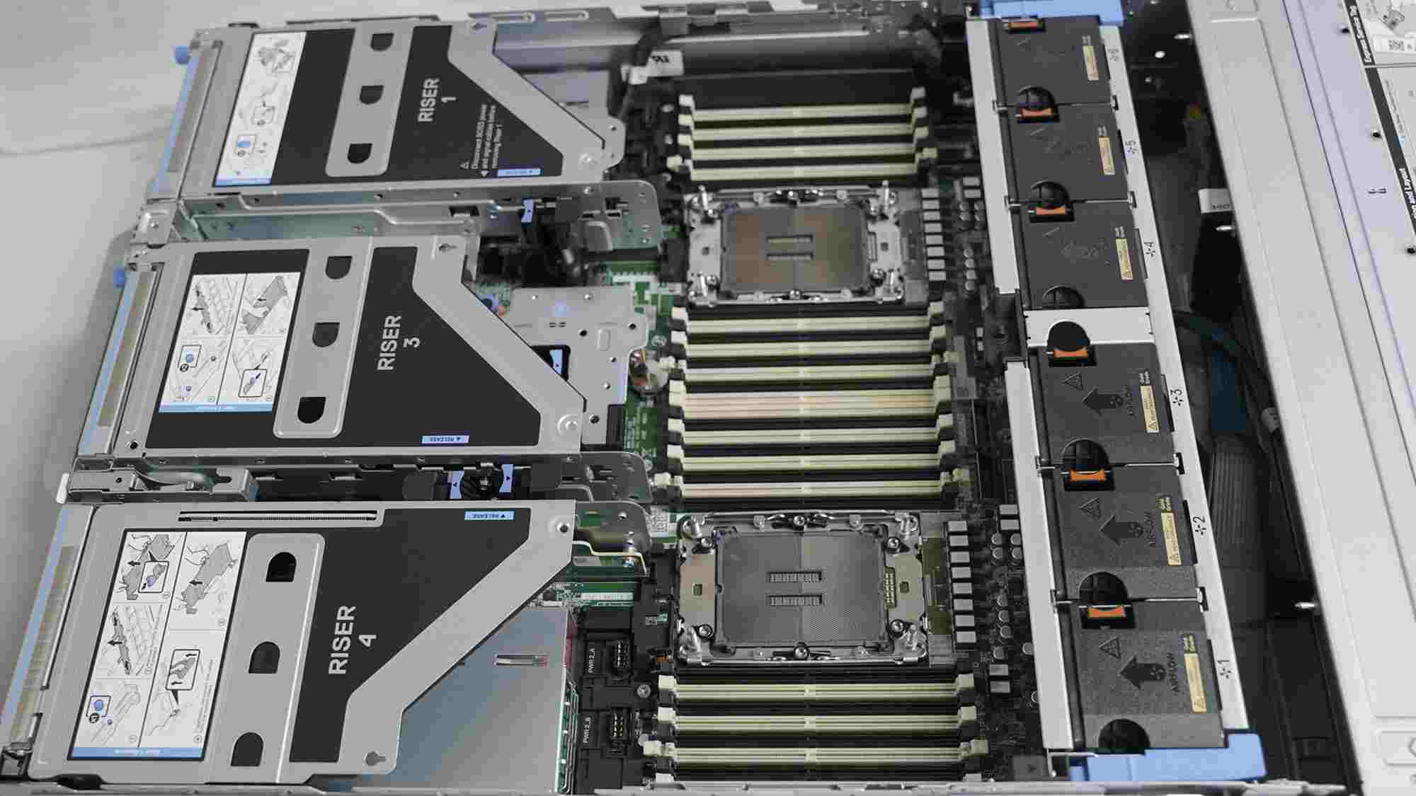
For international buyers, importing PCB assemblies involves several points of potential failure. Our processes are designed to mitigate risk across critical areas:
We source raw laminates directly from verified manufacturers (such as Kingboard and Shengyi). We trace all base aluminum panels, copper foils, and dielectric resins by batch, preventing the use of recycled materials that can cause delamination under thermal cycling.
Our surface finish options include ENIG (Electroless Nickel Immersion Gold), HASL (Lead-Free), and OSP (Organic Solderability Preservatives). Our technical team selects the appropriate option based on your shelf-life and assembly requirements, preventing trace oxidation.
Every batch undergoes testing before packaging, including dielectric breakdown testing, copper peel strength validation, thermal stress tests (solder float testing), electrical open/short circuit flying probe tests, and comprehensive signal/functional analysis.
Technical details for hardware developers and sourcing managers regarding our manufacturing capabilities.
 Velmix