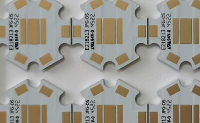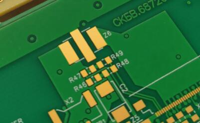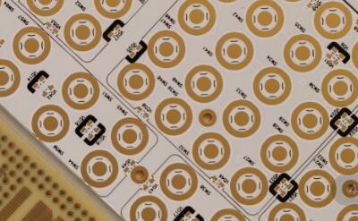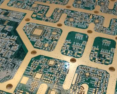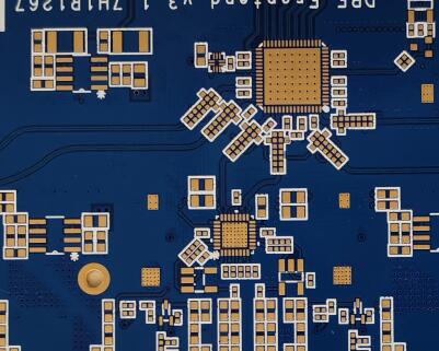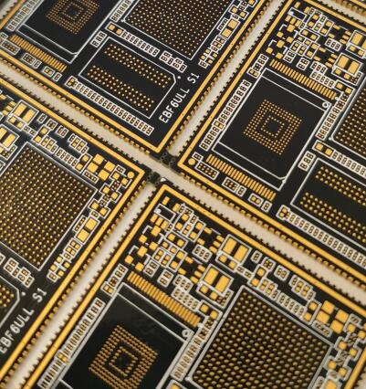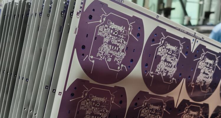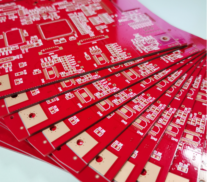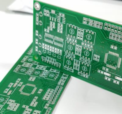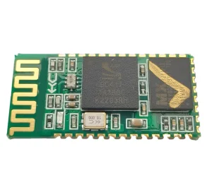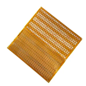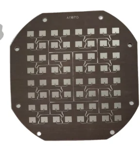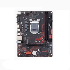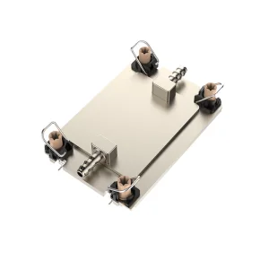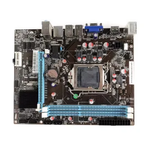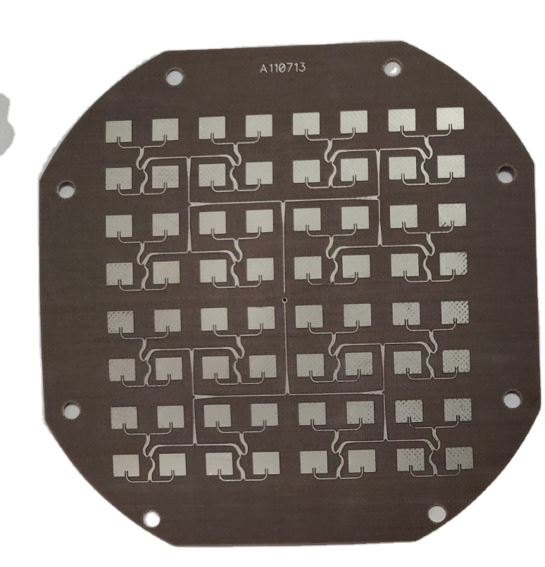
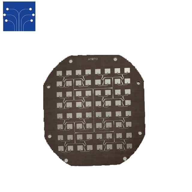
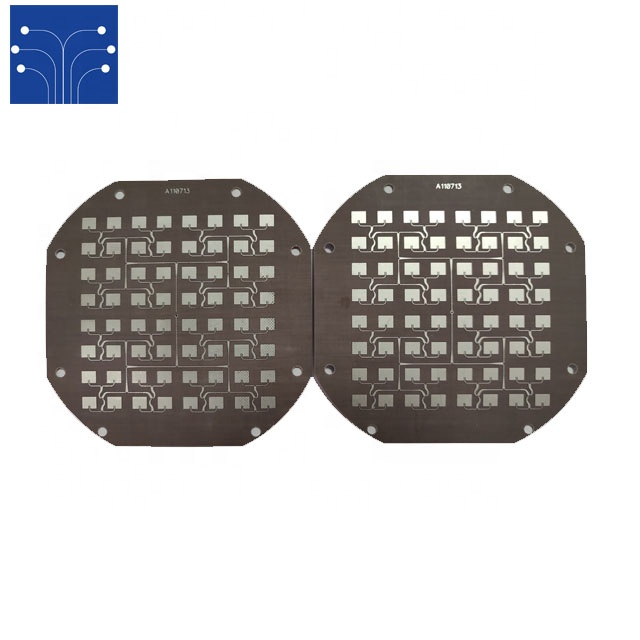
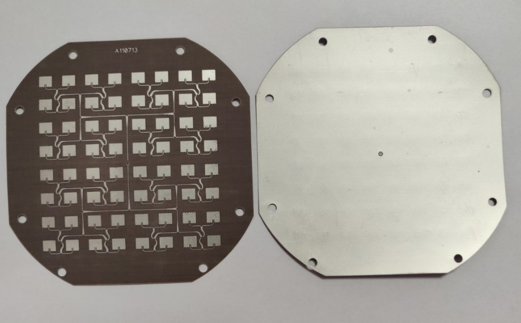
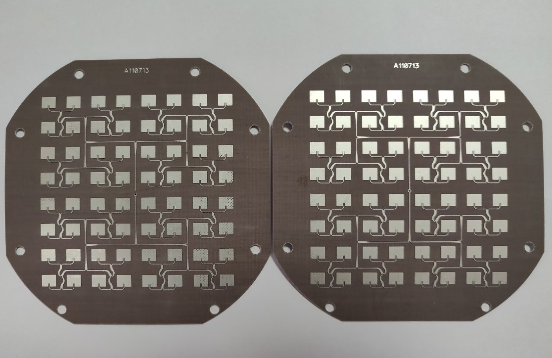
Aluminum substrate PCB circuit board aluminum TOP PCB high-frequency PCB Taconic TLY-5 thickness 0.254 millimeters

Product Description

About Us

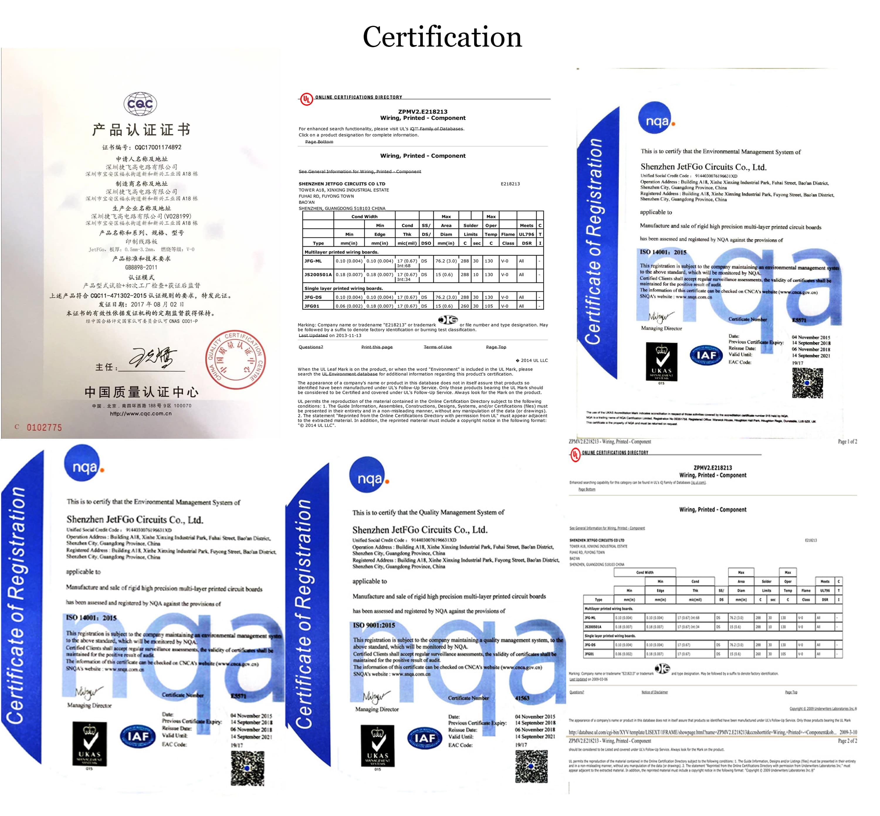
We are a leading manufacturer specializing in high-density multilayer printed circuit boards and specialty boards. With certifications including UL, ISO9001:2015, ISO14001:2015, CQC, IATF16949:2016, and "National Military Standard," we provide top-quality products and services. Our extensive product range includes multilayer boards, impedance boards, high-frequency boards, high TG thick copper foil boards, 5G high-speed boards, buried blind via boards, aluminum-based boards, hybrid dielectric boards, HDI, rigid-flex boards, specialty boards, and customized solutions.

Driven by technological innovation, our products are widely used in industries such as communication equipment, industrial control, automotive electronics, energy and power, medical devices, IoT, research institutions, aerospace, and defense. With over 19 years of experience, we have served over 1,000 technology innovation-oriented enterprises with rapid prototyping and mass production services. We are committed to delivering cutting-edge solutions and exceeding customer expectations in the dynamic electronics industry.

Product Specifications
Model Aluminum substrate
Solder Mask Coverage Resin plug hole
Outer Copper Thickness 0.5oz
Forming Method Mold Forming

Main Products

High-Density Multilayer PCB
Specialty PCB Board
Aluminum PCB Substrate
HDI Rigid-Flex Board
Impedance Control PCB
High Frequency PCB
Thick Copper Foil Board
5G High-Speed PCB Layout
Customized PCB Solution

Production Line and Equipment

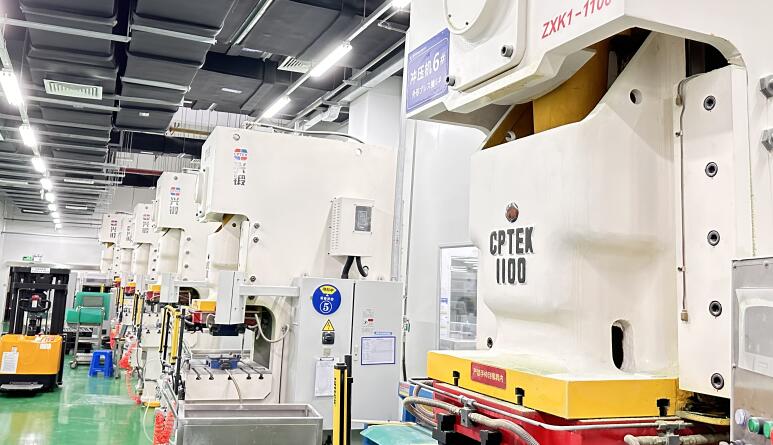
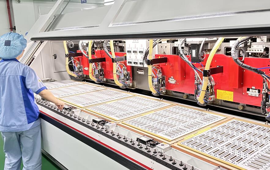
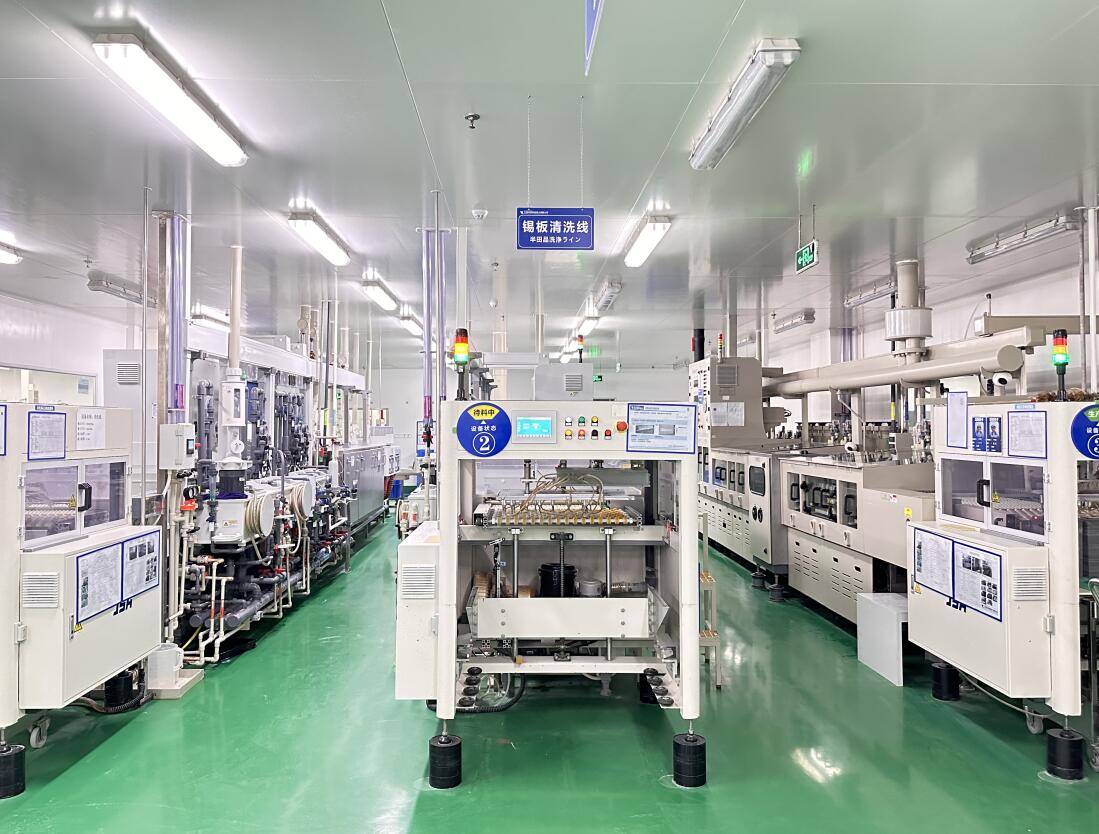
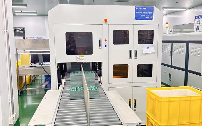
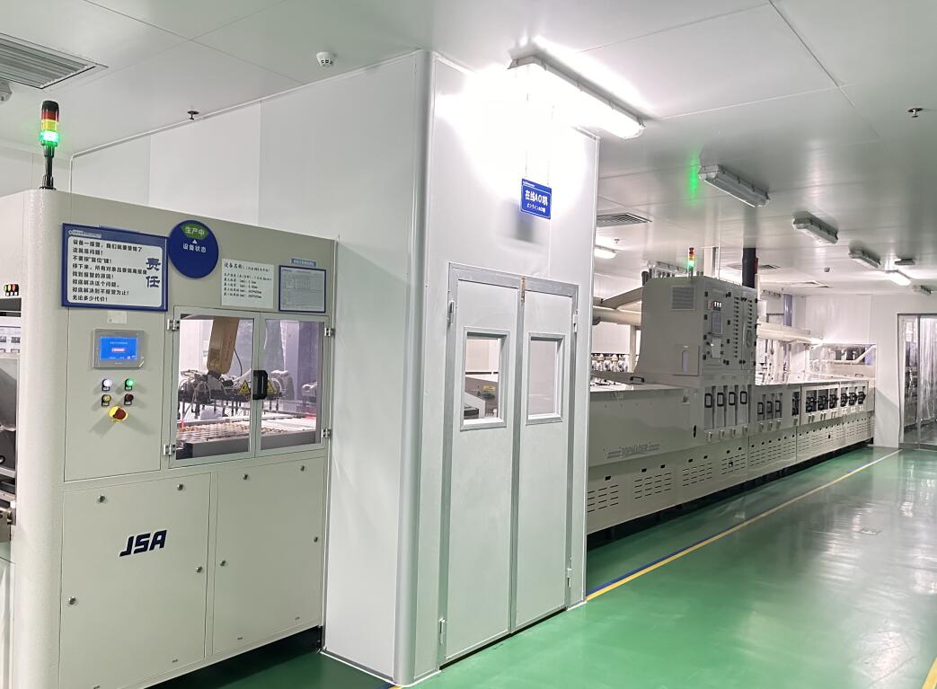
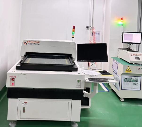
Automated Manufacturing Line
Drilling Equipment
Precision Lamination Station
Advanced Electroplating Process
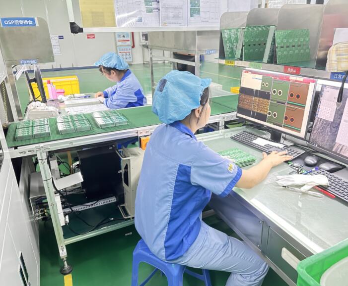
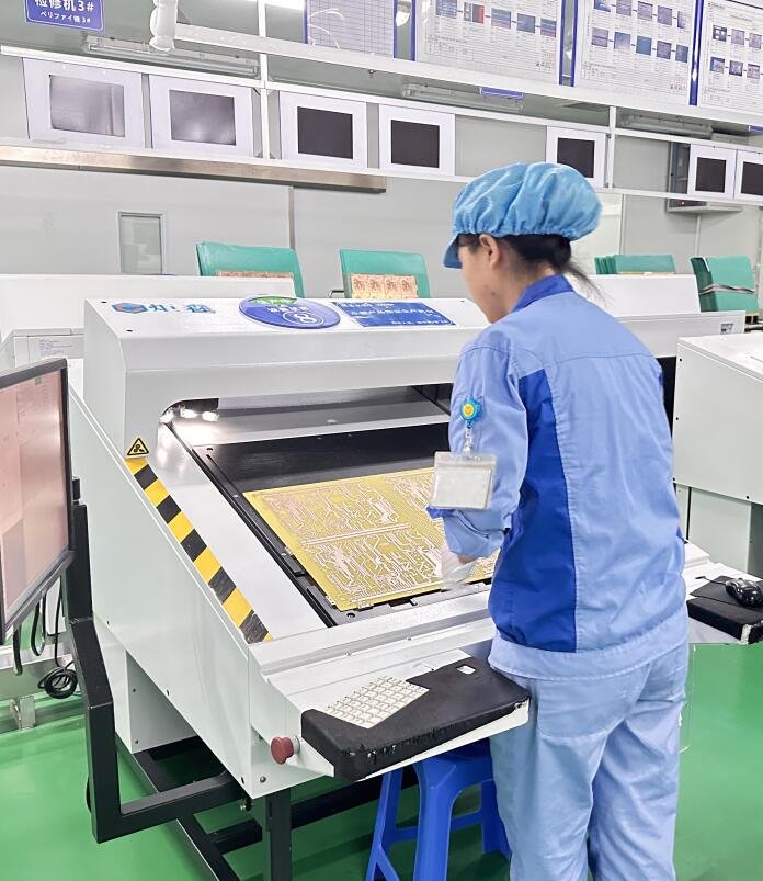
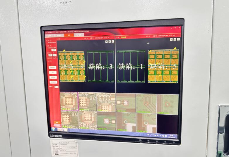
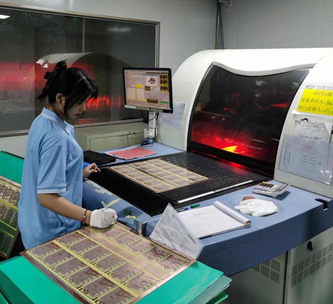
Automatic Optical Inspection
Solder Mask Exposure Machine
Surface Finish Line
CNC Routing and Profiling
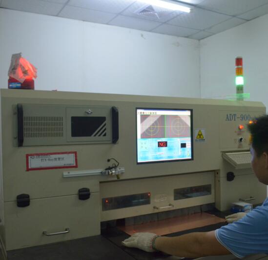
Electrical Testing Area

Manufacturing Technique

Rigid PCB Manufacturing Capability
Category Volume Production Sample Processing
Layer count 1-68L 64 Layer
Max thickness 10mm (394mil) 14mm (551mil)
Min line width/space (Inner layer) 2.2mil/2.2mil 2.0mil/2.0mil
Min line width/space (Outer layer) 2.5mil/2.5mil 2.2mil/2.2mil
Alignment capability (with core board) ±25um ±20um
Alignment capability (Inner layer) ±5mil ±4mil
Max copper 6Oz 30 oz
Holes size (mechanical drilling) ≥0.15mm (6mil) ≥0.1mm (4mil)
Holes size (laser drilling) 0.1mm (4mil) 0.050mm (2mil)
Max size (Unit) 850mm x 570mm 1000mm x 600mm
Max size (Panel) 1250mm x 570mm 1320mm x 600mm
Aspect ratio (Unit) 20:1 28:1
Aspect ratio (Panel) 25:1 35:1
Material (Lead-free/Halogen-free) EM827, 370HR, S1000-2, IT180A, EM825, IT158, S1000 / S1155, R1566W, EM285, TU862HF
Material (High-speed) Megtron6, Megtron4, Megtron7, TU872SLK, FR408HR, N4000-13 Series, MW4000, MW2000, TU933
Material (High-frequency) Ro3003, Ro3006, Ro4350B, Ro4360G2, Ro4835, CLTE, Genclad, RF35, FastRise27
Material (Others) Polyimide, Tk, LCP, BT, C-ply, Fradflex, Omega, ZBC2000
Surface finished HAL, HAL-LF, ENIG, IMMERSION TIN, OSP, IMMERSION SILVER, GOLD FINGER, Hard Gold/Soft Gold Plating
Special technology Blind & buried holes, Via in pad, Semi-plating holes, Counterbore, Step mounting holes, drill Mixed RF PCB, Busbar PCB

Quality Assurance Standards

  • Consciousness of making each product a high-quality product by strictly following the quality management system.
  • Based on ISO 9001, ISO 14001, IATF16949, RoHS, Reach, UL, CQC etc. quality management system. Simultaneously running IATF 16949.
  • Method of involving all staff in the entire process control.
  • Objective and confidence of ensuring 100% quality.
  • Shipping acceptance criteria: Customer requirements, IPC standards.
  • Assisting customers in developing quality standards cooperating with customer experiments to improve product performance.

Laboratory Capabilities

Metallographic Analysis Lab
Reliability Testing Lab
Thermal Stress Testing Equipment
Impedance Test Analysis
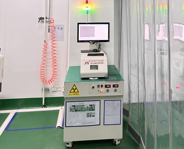
Ionic Contamination Tester

Packing & Shipping

PCB Packaging Process

Shipping Standards

We ship PCB orders with the following flexible options:

  • Air Freight: Fast shipping via UPS, DHL, TNT, CTS, and FEDEX.
  • Railway Freight: Secure overland transport solutions.
  • Seaborne: Cost-effective shipping for bulk orders.
  • Customer Designated: Custom logistics according to your instructions.
Layer Count Sample Shortest Lead Time Sample Standard Lead Time Mass Production Lead Time
2 layer 24 h 3 days 6-7 days
4 layer 36 h 5 days 8-10 days
6 layer 48 h 5 days 8-12 days
8 layer 72 h 5 days 9-12 days
10 layer 4 days 7 days 14 days
12 layer 4 days 7 days 16 days
14 layer 5 days 8 days 16 days
16 layer 5 days 9 days 18 days
18 layer 7 days 10 days 18 days
20 layer and above To be negotiated To be negotiated To be negotiated
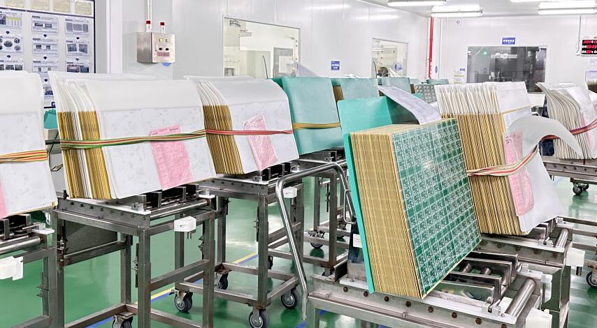
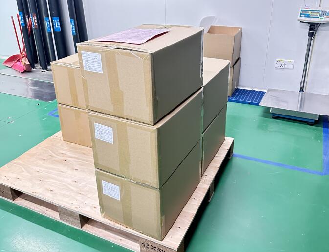
Export Quality Packaging
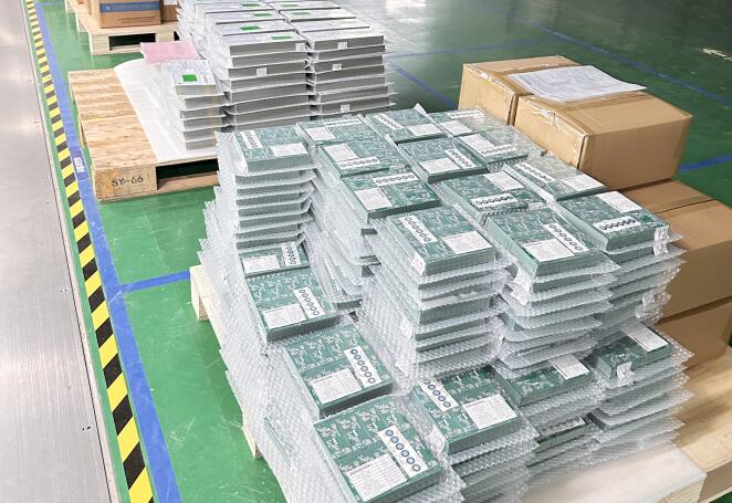
Finished PCB Stack for Delivery

High Efficiency Team

Professional Engineering Team
  • 24h technical support
  • 24h gerber files handling
  • Complete EQ within 4-8 hours
  • Support 400 new project engineering reviews
Accepted CAD/CAM Formats

We process files in the following standard formats:

RS-274-X, RS-274-D CAD, DXP, Protel 99 SE, PADS, GC-CAM
Professional Manufacturing Team
  • All manufacturing processes run 24 hours continuously
  • Monthly production of more than 10K high-mix part numbers
  • Processing over 100 QTA (Quick Turnaround) orders daily
  • One-step comprehensive service from prototype to mass production
Efficient Order Operation Center
  • 24 hours rapid client response
  • Quotations delivered within 4 hours

Certifications

Quality and Environmental Certifications

Frequently Asked Questions

What are your manufacturing capabilities regarding layer counts?
We specialize in 1 to 68 layers for volume production, and can process up to 64 layers for custom engineering samples.
What types of PCB materials do you support?
We support a wide array of advanced materials including lead-free and halogen-free options (EM827, 370HR, S1000-2, IT180A), high-speed materials (Megtron6, Megtron4, Megtron7, TU872SLK), high-frequency materials (Ro3003, Ro3006, Ro4350B, Ro4835), as well as specialty materials like Polyimide, LCP, BT, and C-ply.
What is your shortest lead time for prototype samples?
Our express service offers turnaround times as fast as 24 hours for 2-layer boards, 36 hours for 4-layer boards, and 48 hours for 6-layer boards. Larger multilayer boards (up to 16 layers) can be processed within 5 days.
Which CAD/CAM Gerber file formats do you accept?
We accept standard industry formats including RS-274-X, RS-274-D CAD, DXP, Protel 99 SE, PADS, and GC-CAM files.
What quality management standards are followed during production?
All processes strictly run under ISO 9001, ISO 14001, IATF16949, RoHS, Reach, UL, and CQC quality management guidelines. We ensure 100% quality using IPC standards and customer-specific test criteria.
What shipping options do you offer for orders?
We provide global shipping options including air freight via express carriers (UPS, DHL, TNT, CTS, FEDEX), railway freight, seaborne logistics, or any shipping method designated by the customer.

Related Products