Velmix
1 / 5
| Rigid PCB Manufacturing Capability | |||||
|---|---|---|---|---|---|
| Category | Volume production | Sample processing | |||
| Layer count | - | 1-68L (64 Layer for advanced sample processing) | |||
| Max thickness | - | 10mm (394mil) / 14mm (551mil) | |||
| Min line width/space | Inner layer | 2.2mil / 2.2mil | 2.0mil / 2.0mil | ||
| Outer layer | 2.5mil / 2.5mil | 2.2mil / 2.2mil | |||
| Alignment capability | Alignment with core board | ±25um | ±20um | ||
| Inner layer alignment | ±5mil | ±4mil | |||
| Max copper | 6Oz | 30 oz | |||
| Holes size | Mechanical drilling | ≥0.15mm (6mil) | ≥0.1mm (4mil) | ||
| Laser drilling | 0.1mm (4mil) | 0.050mm (2mil) | |||
| Max size | Unit size | 850mm x 570mm | 1000mm x 600mm | ||
| Panel size | 1250mm x 570mm | 1320mm x 600mm | |||
| Aspect ratio | Unit size | 20:1 | 28:1 | ||
| Panel size | 25:1 | 35:1 | |||
| Material | Lead-free / Halogen-free | EM827, 370HR, S1000-2, IT180A, EM825, IT158, S1000 / S1155, R1566W, EM285, TU862HF | |||
| High-speed material | Megtron6, Megtron4, Megtron7, TU872SLK, FR408HR, N4000-13 Series, MW4000, MW2000, TU933 | ||||
| High-frequency material | Ro3003, Ro3006, Ro4350B, Ro4360G2, Ro4835, CLTE, Genclad, RF35, FastRise27 | ||||
| Others | Polyimide, Tk, LCP, BT, C-ply, Fradflex, Omega, ZBC2000 | ||||
| Surface finished | - | HAL, HAL-LF, ENIG, IMMERSION TIN, OSP, IMMERSION SILVER, GOLD FINGER, Hard Gold / Soft Gold Plating | |||
| Special technology | - | Blind & buried holes, Via in pad, Semi-plating holes, Counterbore, Step mounting holes, Mixed RF PCB, Busbar PCB | |||

| Layer | Sample Shortest lead time | Sample Standard lead time | Mass production lead time |
|---|---|---|---|
| 2 layer | 24 h | 3 days | 6-7 days |
| 4 layer | 36 h | 5 days | 8-10 days |
| 6 layer | 48 h | 5 days | 8-12 days |
| 8 layer | 72 h | 5 days | 9-12 days |
| 10 layer | 4 days | 7 days | 14 days |
| 12 layer | 4 days | 7 days | 16 days |
| 14 layer | 5 days | 8 days | 16 days |
| 16 layer | 5 days | 9 days | 18 days |
| 18 layer | 7 days | 10 days | 18 days |
| 20 layer and above | To be negotiated | To be negotiated | To be negotiated |
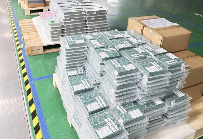
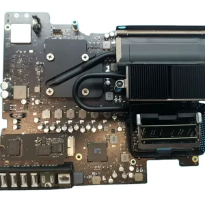
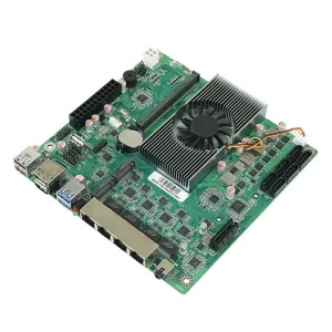
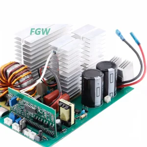
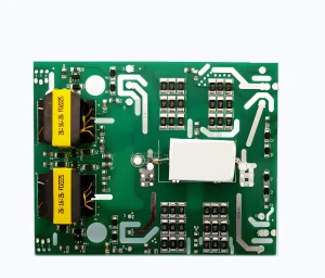
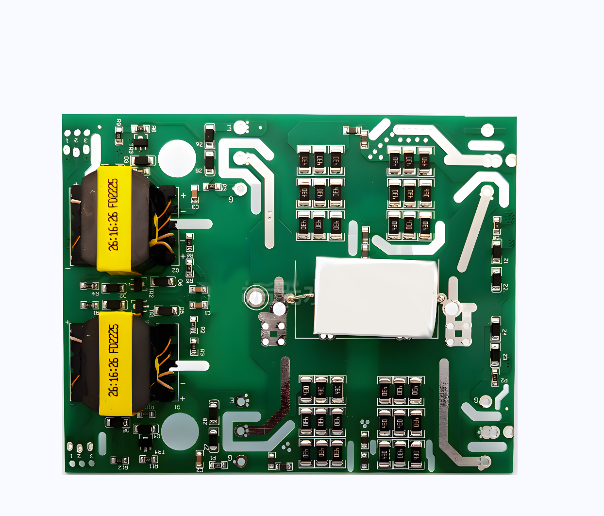
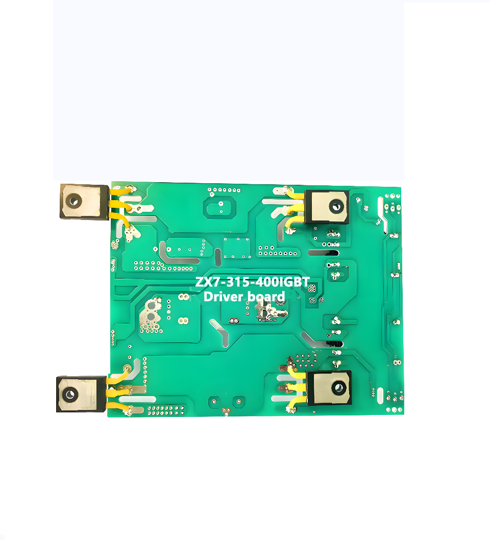
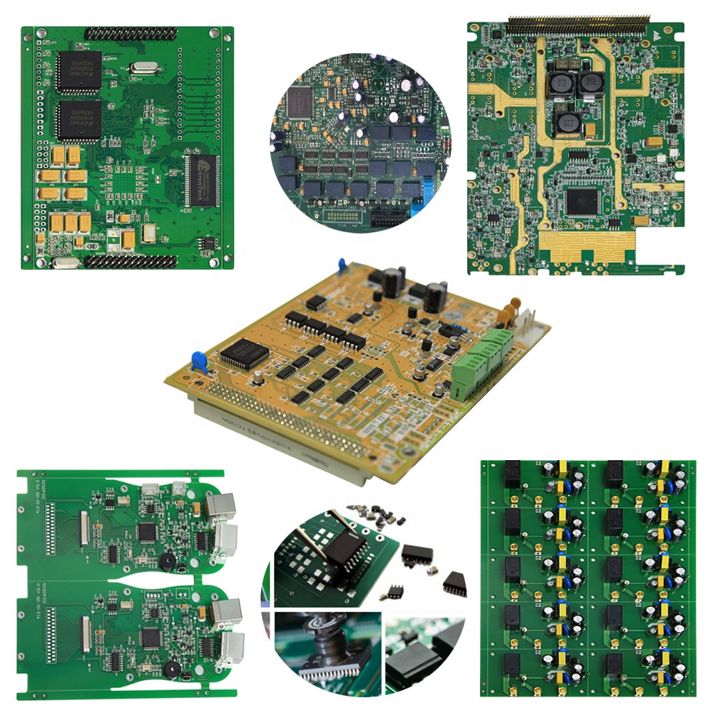
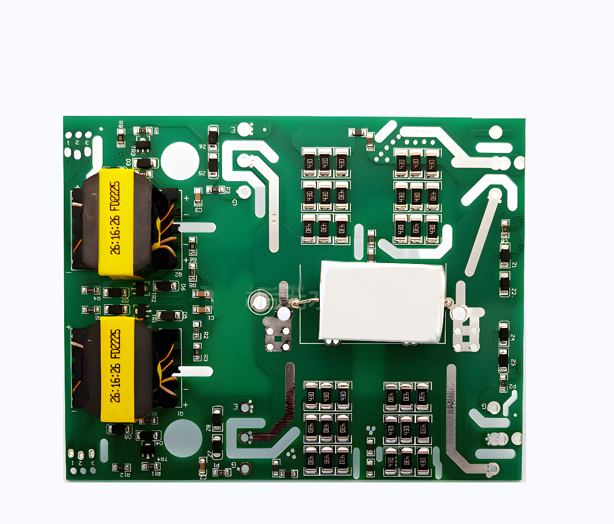
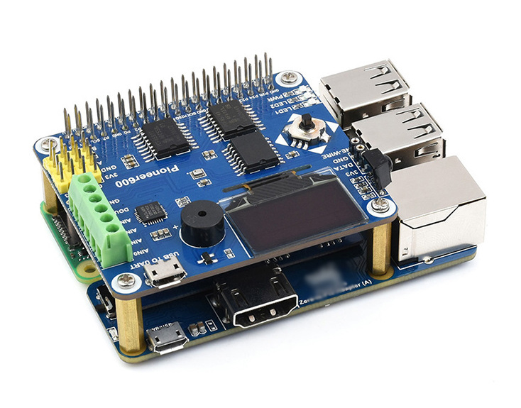
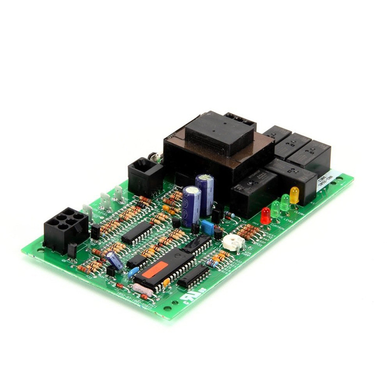
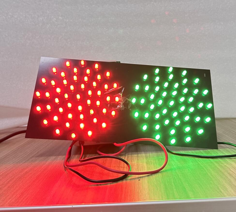
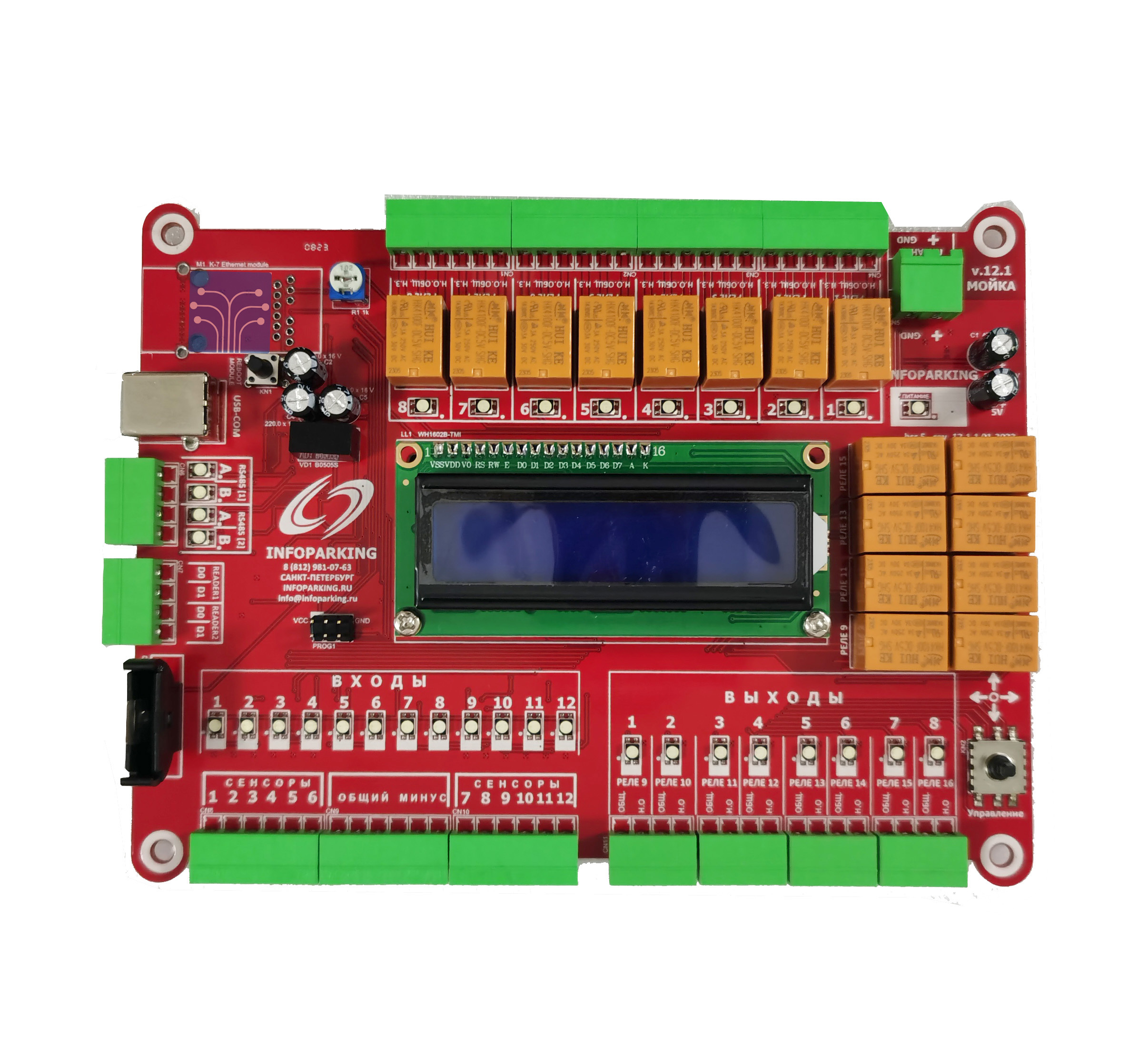
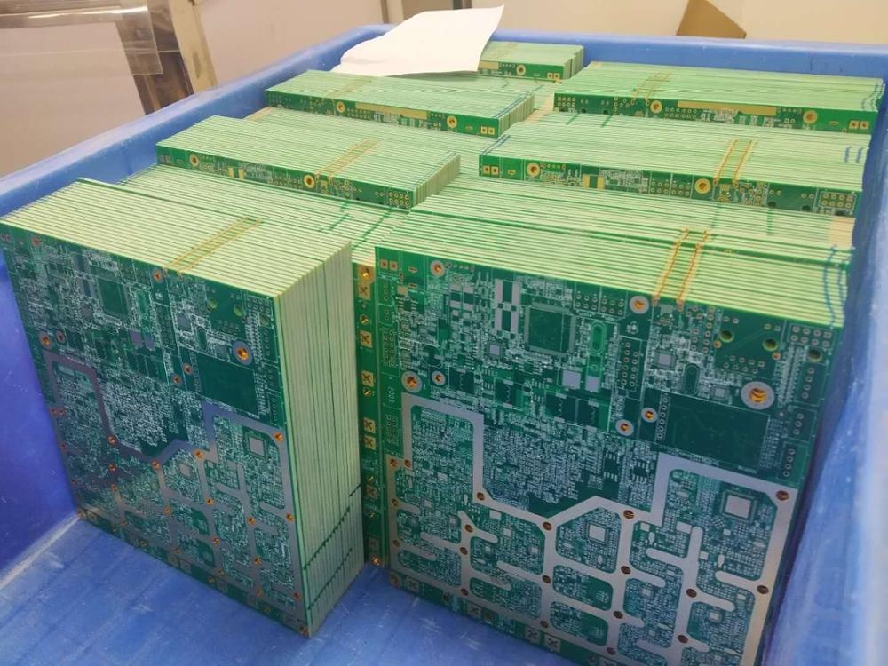
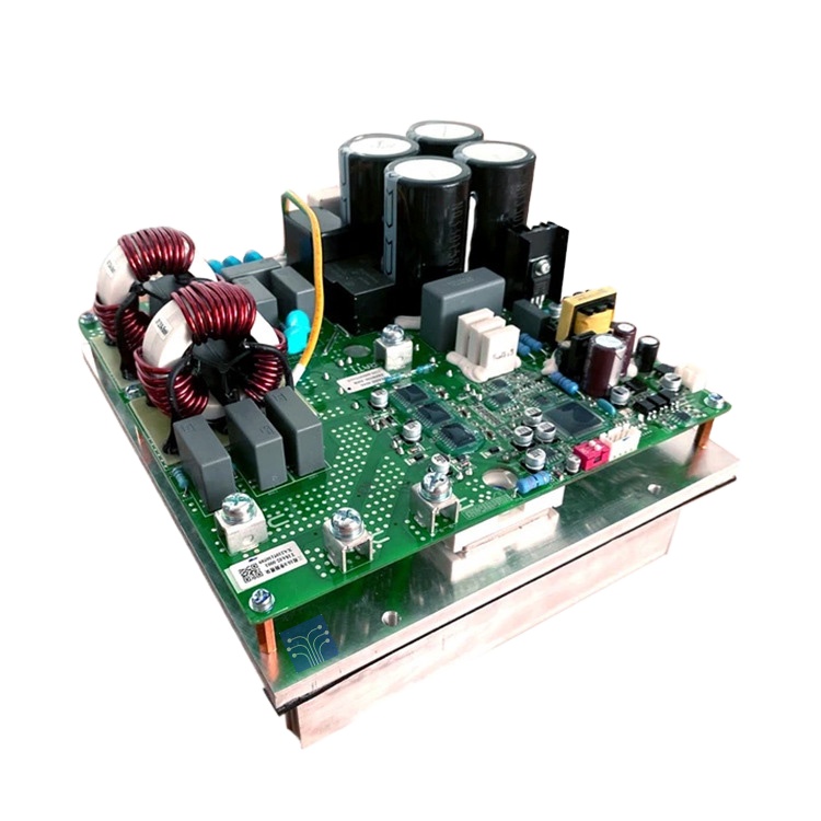
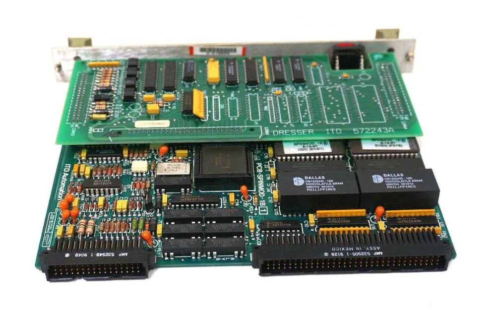
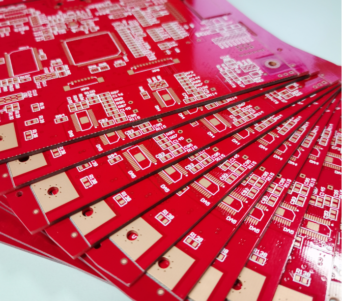
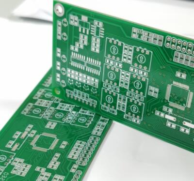
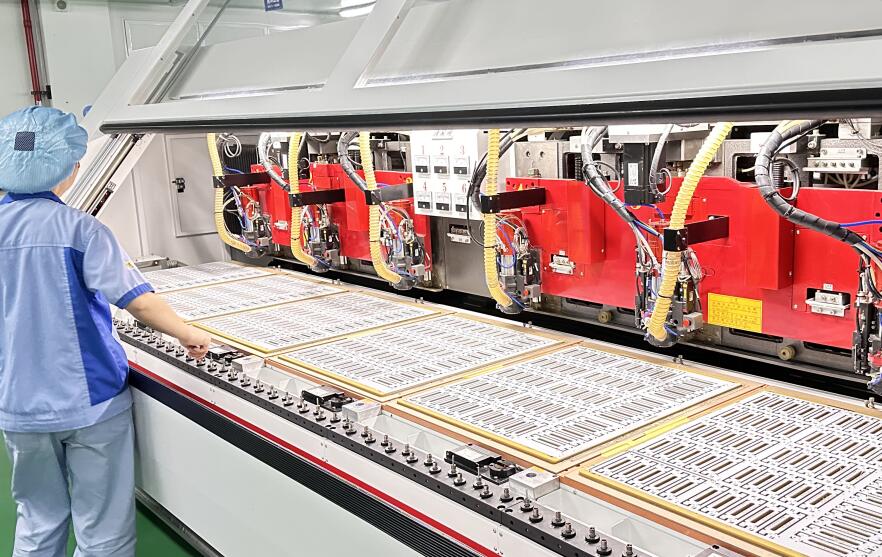
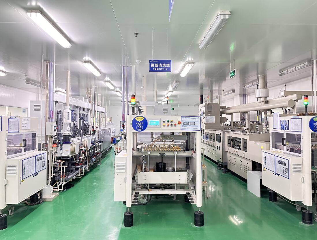
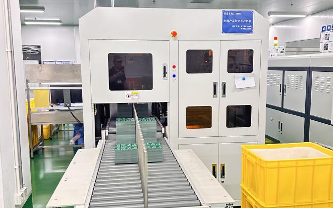
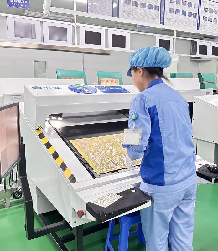
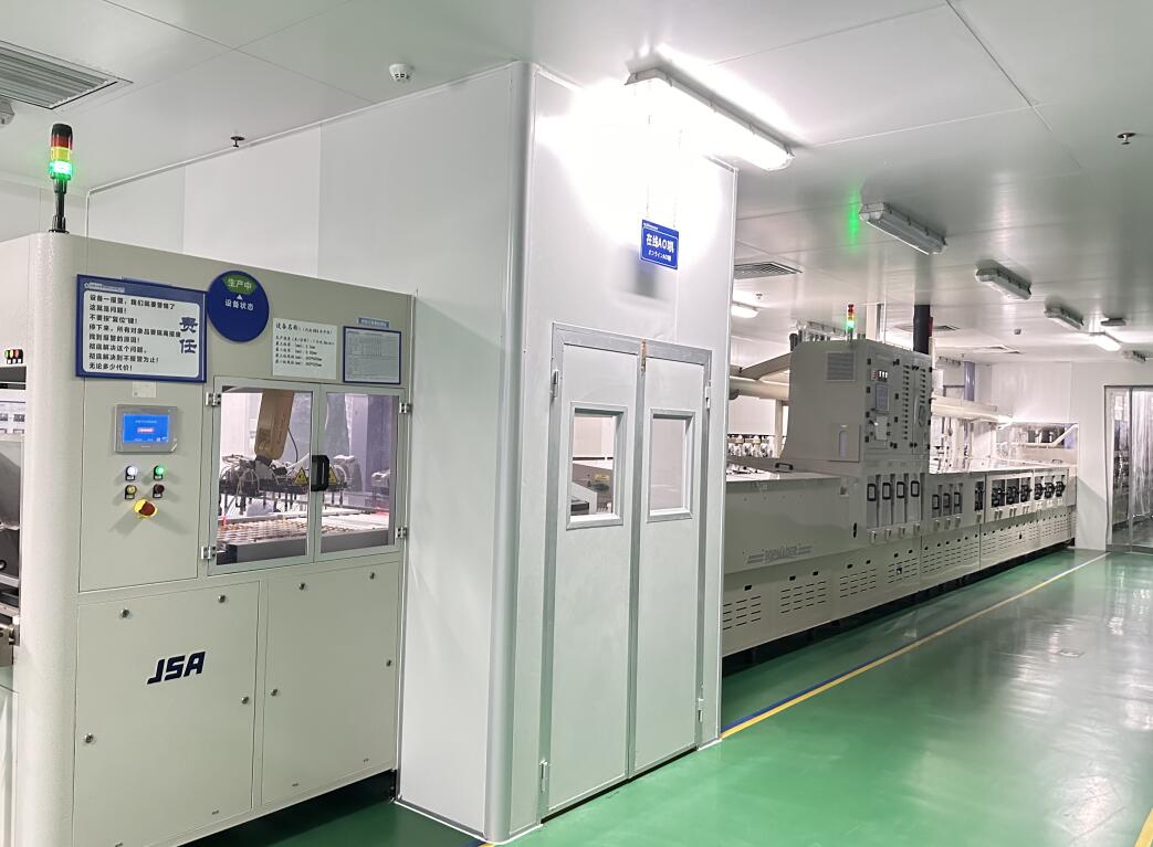
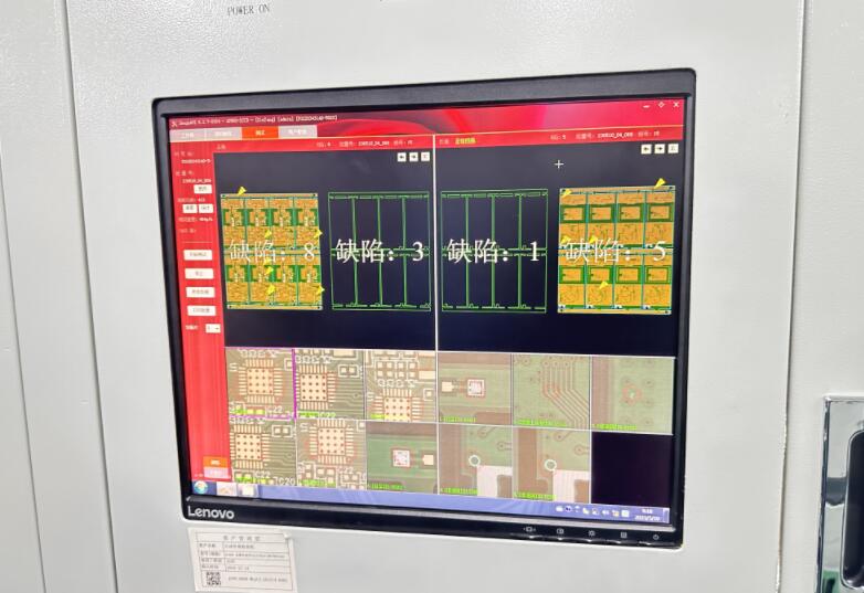
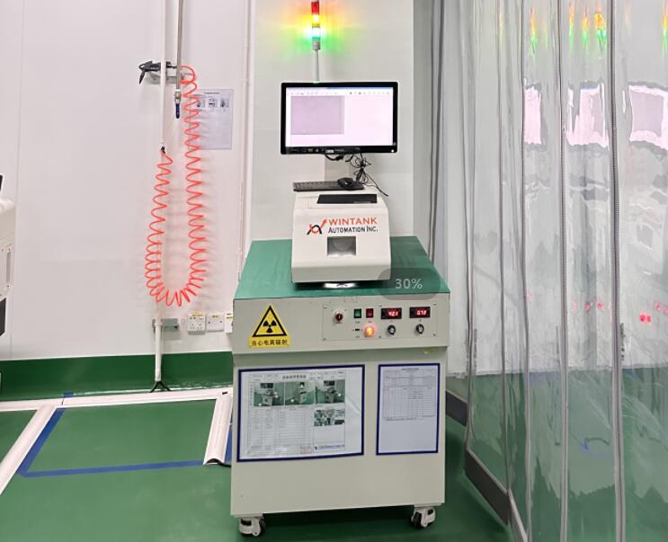
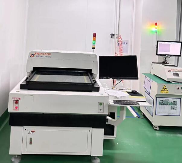
We manufacture a wide range of PCBs, including high-density multilayer boards (1-68 layers), impedance boards, high-frequency boards, high TG thick copper foil boards, 5G high-speed boards, buried blind via boards, aluminum-based boards, hybrid dielectric boards, HDI, rigid-flex boards, and other specialty customized solutions.
Lead times depend on the layer count. For 2-layer PCBs, the shortest sample lead time is 24 hours, with standard delivery in 3 days, and mass production in 6-7 days. For multilayer PCBs (4-18+ layers), samples range from 36 hours to 7 days, and mass production takes between 8 and 18 days.
We accept standard industry formats, including RS-274-X and RS-274-D (Gerber formats), CAD, DXP, Protel 99 SE, PADS, and GC-CAM files.
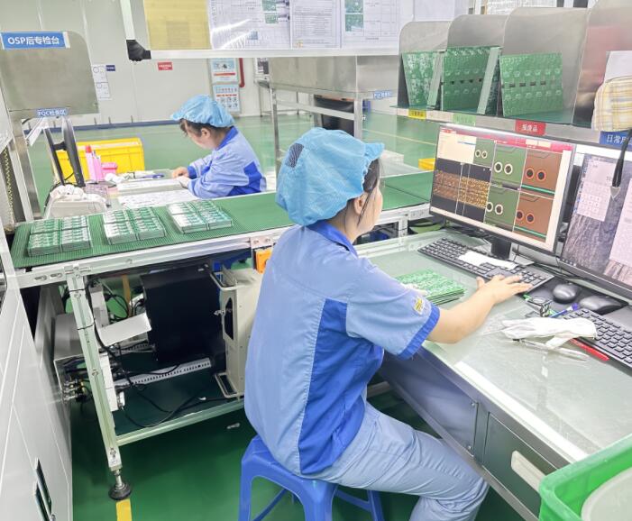
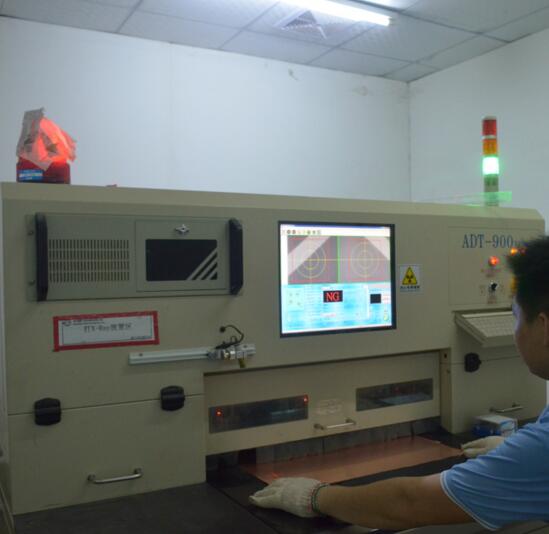
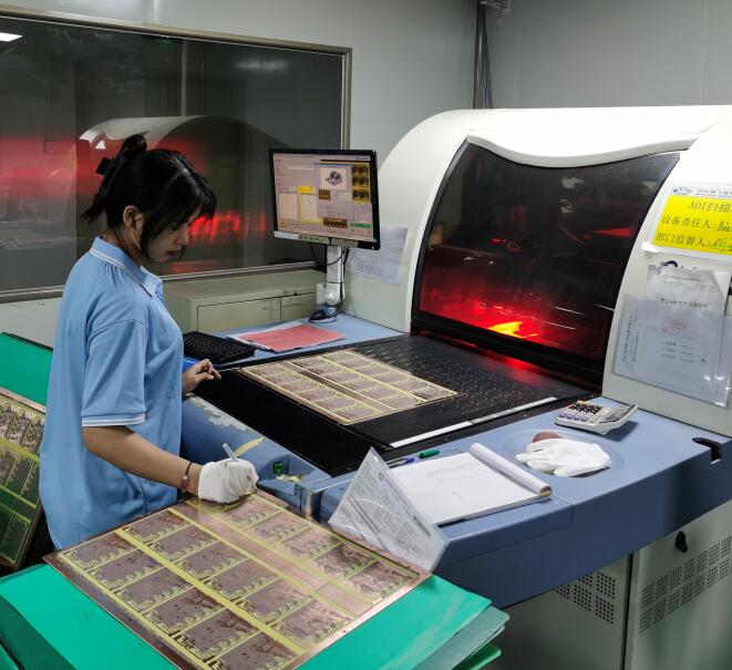
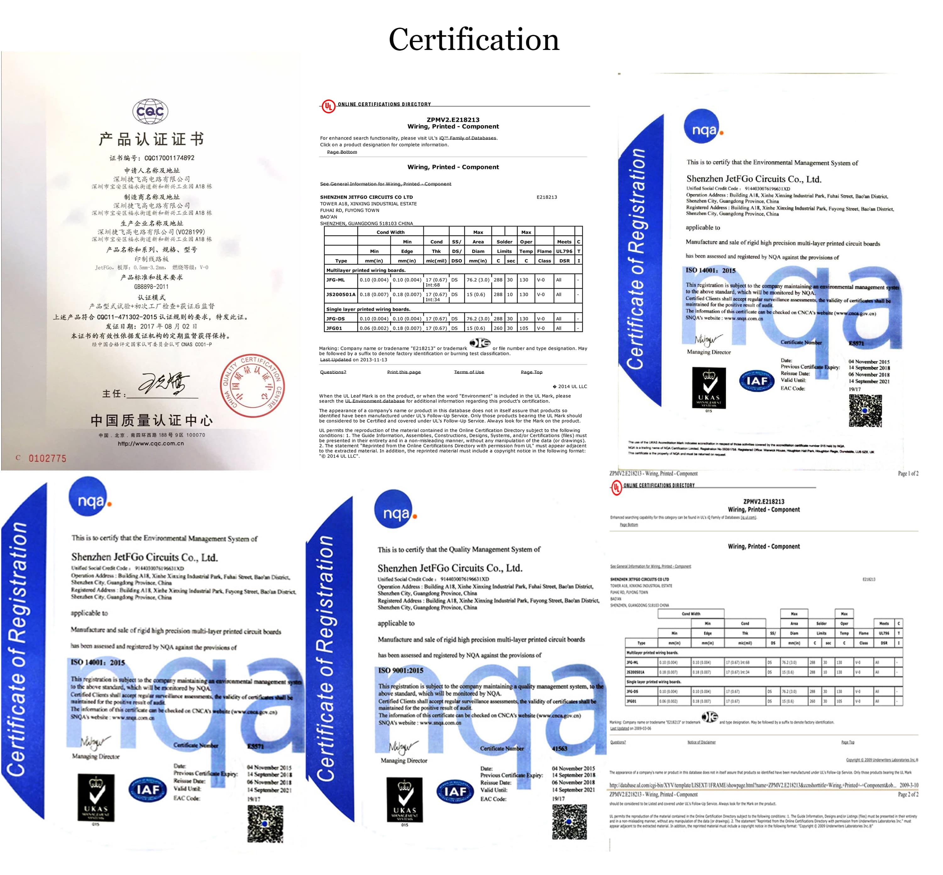
Our manufacturing processes strictly conform to quality management systems certified by UL, ISO9001:2015, ISO14001:2015, CQC, and IATF16949:2016. Shipping acceptance criteria follow customer requirements and IPC standards.
Because PCBs are custom-manufactured products, standard returns and exchanges are not supported. For quality-related issues, please contact customer service immediately for a refund or replacement support. Compensation does not cover losses beyond the product value.
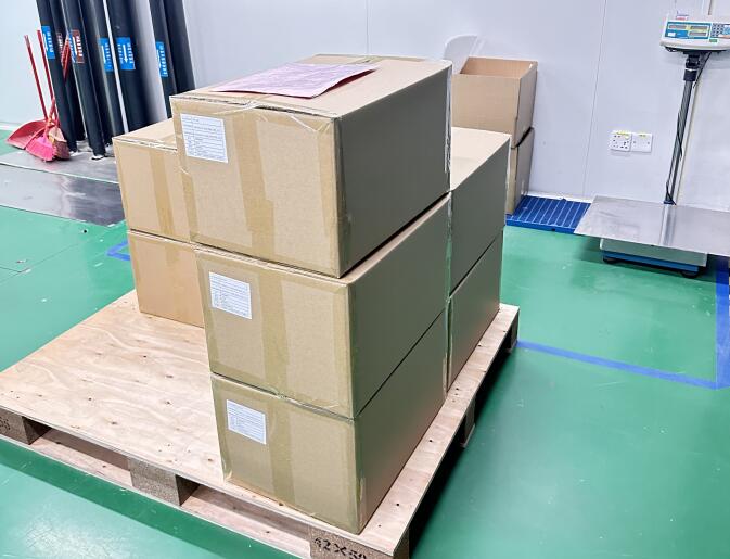
We provide several shipping options based on customer preference: Air express delivery (UPS, DHL, TNT, CTS, and FEDEX), railway freight, seaborne shipping, or any other customer-designated shipping carrier.