As the geopolitical and economic hub of the region, Moscow and its surrounding industrial sectors (including Zelenograd's microelectronics cluster and Technopolis Moscow) have experienced a significant transformation. Modernization of the electric grid, high-speed rail networks, and localized heavy industrial machinery manufacturing have increased the technical demands on printed circuit board (PCB) architecture. Traditional FR4 PCBs with standard 1oz (35µm) copper foil are no longer adequate for handling high currents and managing severe thermal loads.
Thick Copper PCBs (defined as boards with copper cladding of 3oz/ft² to 10oz/ft² or more) serve as the structural and electrical backbone for power supplies, traction motor drives, military-grade telecommunications, and high-capacity transformer stations. In Moscow's sub-zero winter environments, electronics must operate under severe temperature fluctuations. The differential thermal expansion between the copper traces and substrate material (typically high-Tg FR4 or polyimide) requires precise engineering to prevent trace delamination, solder joint fatigue, and dielectric breakdown.
Heavy copper layers function as integrated heat sinks. In sub-zero Moscow operations, our specialized thick copper laminates disperse localized heat spots across the entire board substrate, reducing failure rates in remote power grids and railway control interfaces.
Globally, the electronic manufacturing services (EMS) sector is witnessing a shift toward power integration. The proliferation of electric vehicles (EVs), renewable energy conversion systems (such as solar inverters and wind turbine pitch controls), and high-output computing platforms (AI data center power distribution units) has elevated heavy copper PCB demand. According to recent industrial data, the CAGR of high-power PCBs is outperforming standard multilayer variants, driven by the necessity to combine control circuits and high-current circuits on a single board (often called "heavy copper embedded technology").
International procurement departments are prioritizing manufacturing partners capable of maintaining precise trace dimensions. Fabricating thick copper requires specialized chemical etching controls. Without advanced equipment, thick traces suffer from "undercutting," which compromises the current-carrying capability and creates critical resistance anomalies. Velmix Technology coordinates with global component networks to deliver heavy copper substrates that satisfy international safety codes, including UL 746C and IPC-6012 Class 3 requirements.
Deploying robust circuitry for high-reliability systems worldwide. Our production metrics demonstrate our commitment to process control and precision engineering.
For Moscow-based industrial enterprises, sourcing thick copper PCBs from Shenzhen-based factories like Velmix Technology presents key efficiency and supply chain benefits:
Every batch of thick copper boards destined for Moscow undergoes cross-section analysis, solderability testing, and thermal stress testing to ensure the copper barrel plating maintains integrity under continuous high-temperature loads.
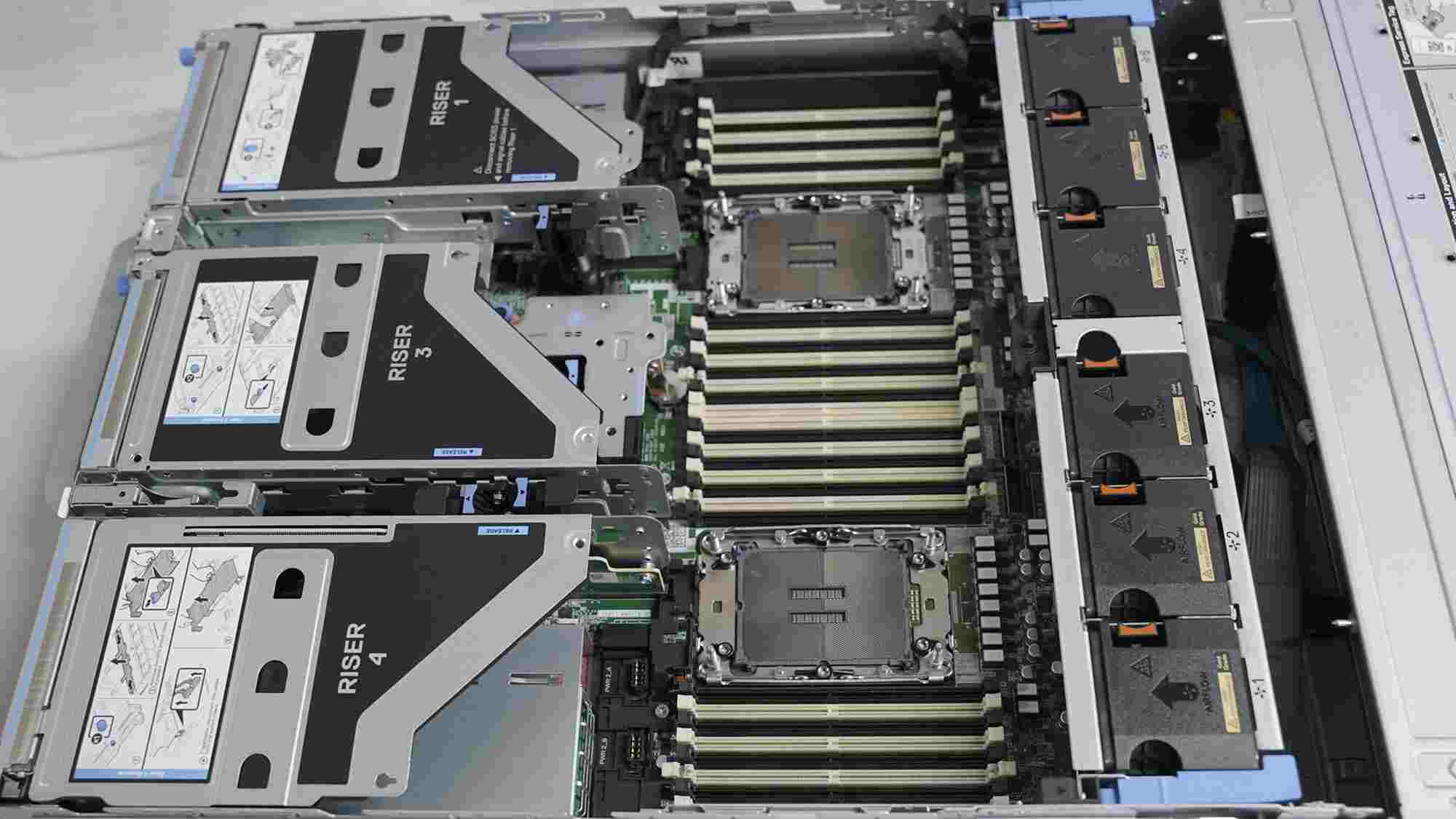
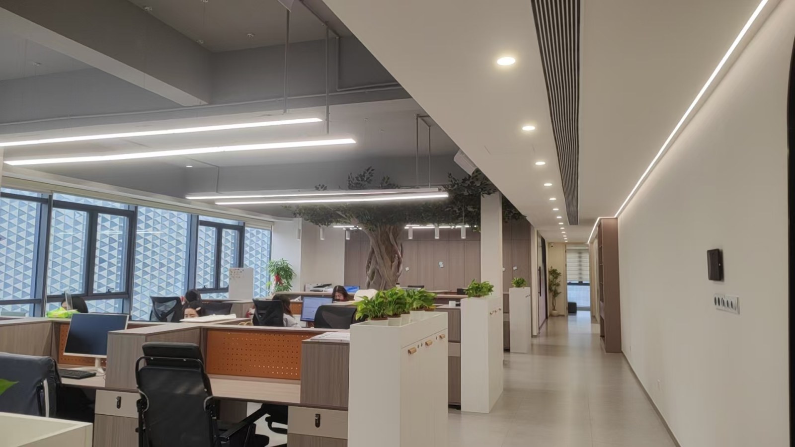
Velmix Technology Co., Ltd. is a specialized electronics developer and PCBA manufacturer located in Shenzhen, China. Since 2017, we have worked with global distributors, brand owners, and industrial enterprises to deliver robust solutions for computing, power electronics, and server cooling systems.
| Technical / Operational Category | Detailed Specifications & QC Parameters |
|---|---|
| Company Name | Velmix Technology Co., Ltd. |
| Established / Export History | Established 2017 | 8 Years Export Experience | 15 Years Industry Experience |
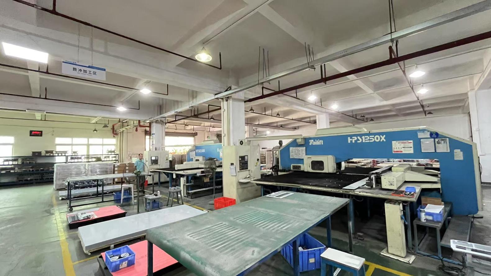
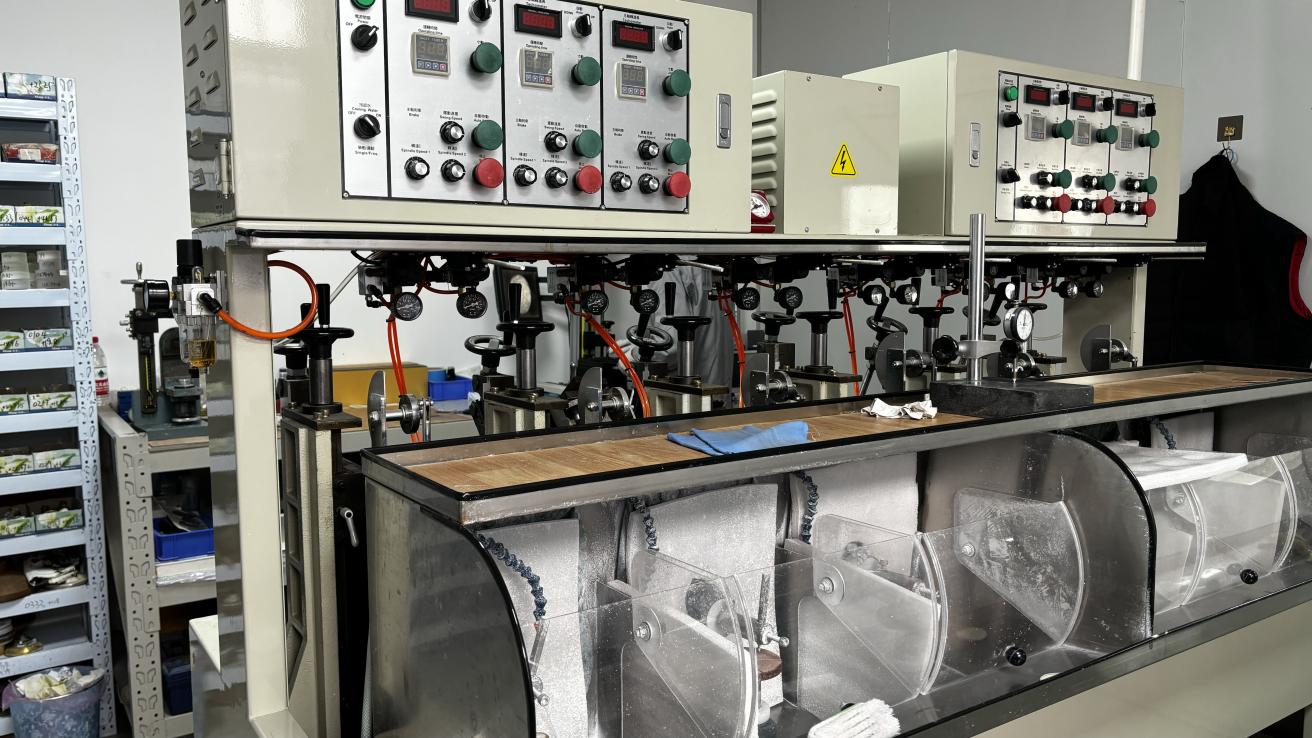
| Manufacturing Facility Area | 368㎡ Cleanrooms and Advanced Assembly Space |
| Copper Thickness Range | From standard 1oz up to extreme 12oz (Heavy/Thick Copper) |
| Testing & Qualification | 100% Inspection via AOI, Flying Probe, Signal Integrity, and Thermal Burn-in Tests |
| Personnel Composition | 84 R&D Engineers & 56 Quality Control Staff |
| Customization Options | OEM/ODM, custom copper weights, selective plating, thermal baseplates |
| Annual Export Revenue | USD 18.6 Million (Serving Europe, Middle East, North & South America) |

Understanding how thick copper PCBs interface with local Moscow hardware designs helps clarify the engineering decisions required during the design phase:
Substation monitoring modules operating in the Moscow Oblast require high-voltage insulation and high-current capacity. Utilizing 4oz copper traces on a metal-clad base allows these transducers to withstand momentary line-surge events without trace failure, preventing localized brownouts.
Railway systems running through Moscow transit corridors rely on motor control inverters that switch hundreds of amperes. By using selective heavy copper (combining 2oz signal traces with 6oz power paths on the same board layer), developers can eliminate external wire harnesses and reduce the overall physical volume of the control box.
The processing centers near Moscow handling big data arrays require efficient power delivery units (PDUs). Heavy copper PCBs reduce trace resistance and power loss ($I^2R$), directly translating to reduced operating costs and lower demands on HVAC infrastructure.


Submit your Gerber files and electrical parameters. Our thermal management engineers will review your trace layout and provide a manufacturing feedback assessment within 24 hours.
Send Inquiry Now Velmix