Optimized electronic components, assemblies, and custom design kits serving Sydney's defense, aerospace, and medical engineering standard lines.
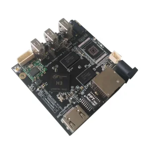
The Greater Sydney region is undergoing a major renaissance in advanced electronics design and manufacturing. From the innovation centers of Macquarie Park and Silverwater to the emerging high-tech zones of the Western Sydney Aerotropolis, local tech companies, defense contractors, medical device designers, and hardware startups require precision prototype-to-volume manufacturing capabilities.
Surface Mount Technology (SMT) forms the backbone of these local facilities. A key component of reliable solder paste deposition is the laser-cut stencil. As local SMT assembly operations shift towards ultra-miniaturized form factors, like 0201/01005 passives and micro-BGAs, the demands on stencil aperture geometry, roughness, and position accuracy have risen exponentially.
Velmix Technology Co., Ltd. addresses this vital market. We specialize in supplying high-fidelity laser-cut SMT stencils, high-temperature PCB prototypes, and thermal cooling modules designed to match the stringent quality levels demanded by Sydney's premium manufacturers. Our custom laser-etched stencils provide the necessary dimensional tolerances to keep solder bridge defects to absolute zero.
Understanding the critical variables of SMT stencil design and mechanical parameters to optimize line yield.
For optimal paste release, the stencil design must respect standard IPC-7525 guidelines. Specifically, the Area Ratio (aperture opening area divided by aperture wall area) must be greater than 0.66. Our automated CAD/CAM validation team cross-checks all customer designs before cutting, preventing printing failure on fine-pitch components.
Utilizing high-end LPKF laser cutting machines running optimized fiber lasers, we achieve positioning accuracies within ±2μm and repeatability of ±1μm. This ensures that multicavity arrays on multi-up SMT boards have perfect registration across the entire active print region.
We offer optional micro-polishing and hydrophobic Nano-coating. Nano-coatings dynamically reduce the frequency of under-stencil cleaning cycles on the print line, reducing paste build-up, decreasing assembly line downtime, and preventing bridge defects on QFN leads.
Navigating global semiconductor and component shortages requires a robust, agile logistics pipeline. By locating our production hub in Shenzhen, China—the electronics capital of the world—Velmix Technology is uniquely positioned to source high-grade raw components, advanced PCB layers, and custom-tensioned steel frames, and package them for rapid export to Sydney.
We work closely with major express carriers (DHL, FedEx, UPS) to run custom clearances smoothly. Our export team ensures that all shipments carry proper HTS documentation (Harmonized Tariff Schedule code for laser stencils and PCBs) to avoid port delays, giving Sydney engineers an end-to-end delivery guarantee. With local SMT lines running 24/7, our 3-5 days transit from Shenzhen represents a massive time and cost advantage over domestic boutique suppliers.
| Phase | Process Detail | Timeframe |
|---|---|---|
| 1. DFM Check | CAD Gerber data review & aperture optimization | 2-4 Hours |
| 2. Laser Cut | Laser fiber cutting & post-polishing | 4-8 Hours |
| 3. Quality QC | Aperture dimensions inspection & Tension check | 1 Hour |
| 4. Packaging | Vacuum sealed & shockproof wooden casing | 2 Hours |
| 5. Shipping | Air express to Sydney (SYD Terminal) | 3-4 Days |
A professional high-performance memory and hardware solutions manufacturer.
Velmix Technology Co., Ltd. is a professional DDR5 memory manufacturer based in Shenzhen, China, specializing in the research, development, production, and global distribution of high-performance DRAM memory solutions. Since its establishment in 2017, Velmix has been committed to delivering reliable, high-speed memory products for consumer electronics, industrial applications, gaming systems, servers, and embedded computing.
Operating from a modern manufacturing facility covering 368㎡, we combine advanced production technologies with strict quality management to ensure every memory module meets international performance and reliability standards. Our experienced engineering team continuously develops innovative DDR5 memory solutions to meet the evolving demands of AI computing, edge devices, cloud infrastructure, and next-generation computing platforms.
Today, Velmix serves customers in more than 40 countries and regions, offering flexible OEM and ODM manufacturing services for global brands, distributors, system integrators, and industrial equipment manufacturers. By focusing on product consistency, fast delivery, and technical innovation, we have built long-term partnerships across Europe, North America, Southeast Asia, and the Middle East.
| Item | Information Details |
|---|---|
| Company Name | Velmix Technology Co., Ltd. |
| Established | 2017 |
| Facility Area | 368㎡ |
| Annual Export Revenue | USD 18.6 Million |
| Export Experience | 8 Years |
| Industry Experience | 15 Years |
| Quality Control | 100% Full Inspection Before Shipment |
| Product Inspection Methods | Signal Integrity Test, Burn-in Test, Compatibility Test, Functional Test & Random Sampling |
| QC Staff | 56 Employees |
| Business Type | Manufacturer & Exporter |
| Main Markets | North America, Europe, Southeast Asia, Middle East & South America |
| Supply Chain Partners | 986+ |
| Main Customer Types | Brand Owners, OEM Manufacturers, System Integrators, Distributors & Wholesalers |
| R&D Capability | Independent Product Design, PCB Development & Firmware Optimization |
| Customization Options | OEM, ODM, Private Label, Customized Capacity, Heat Spreader, PCB Color & Packaging |
| New Products Launched Last Year | 138 Models |
| R&D Engineers | 84 Engineers |
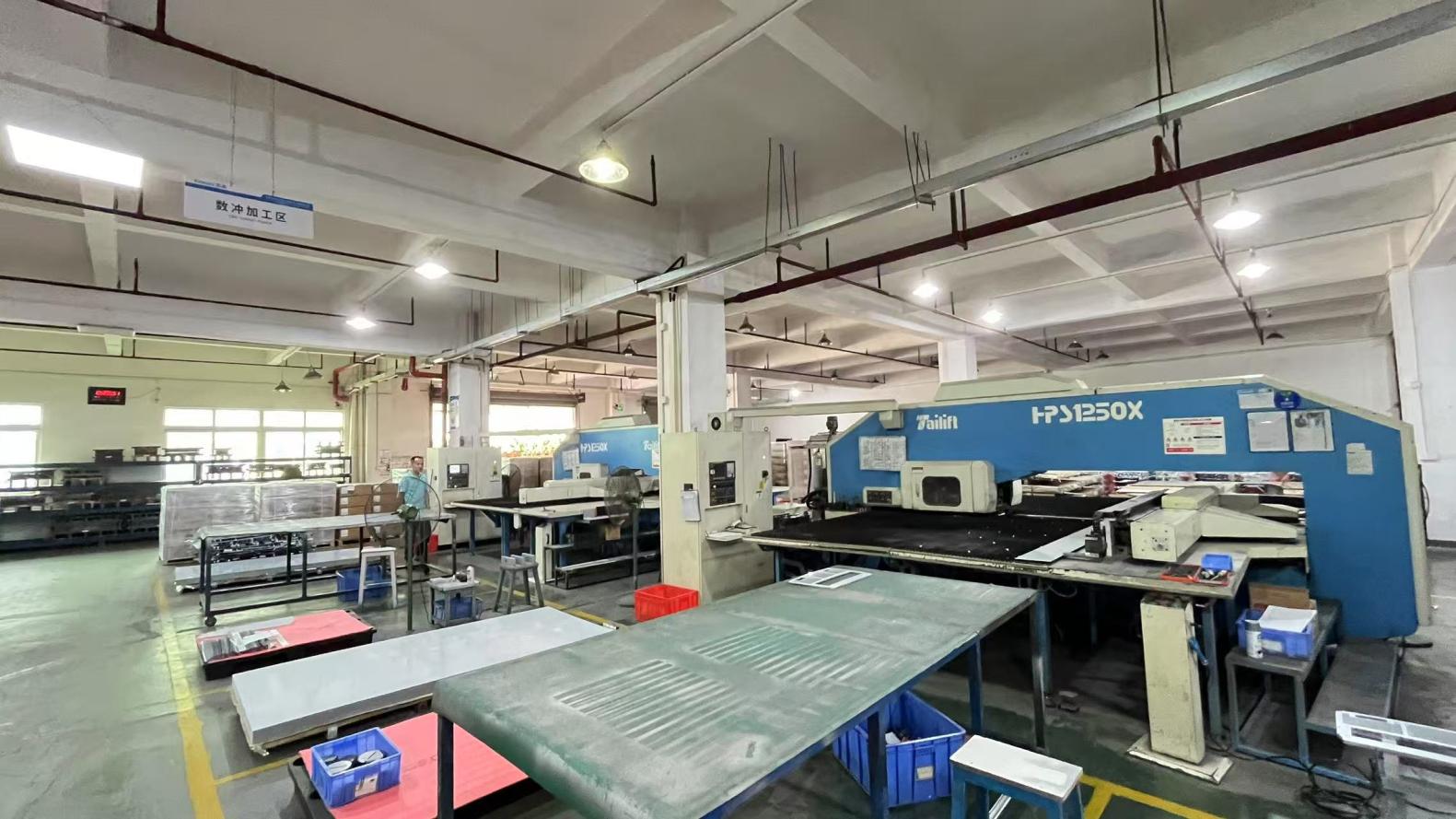

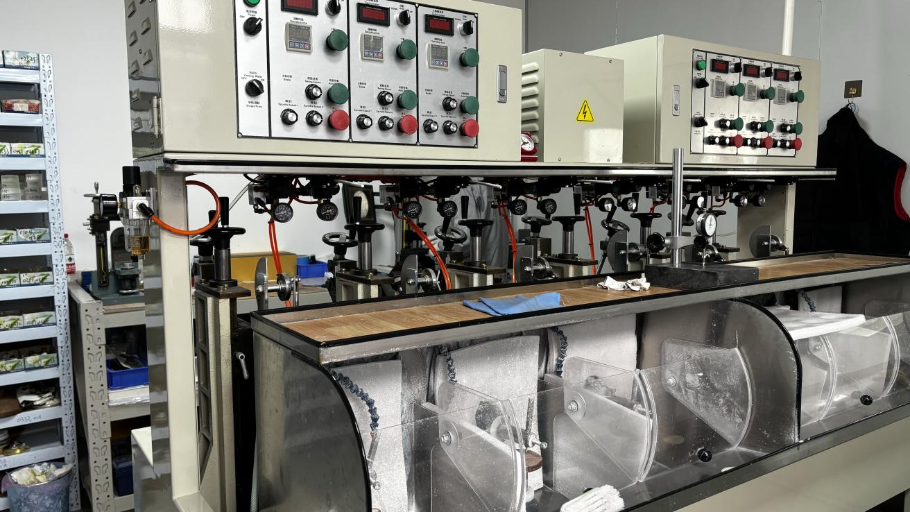
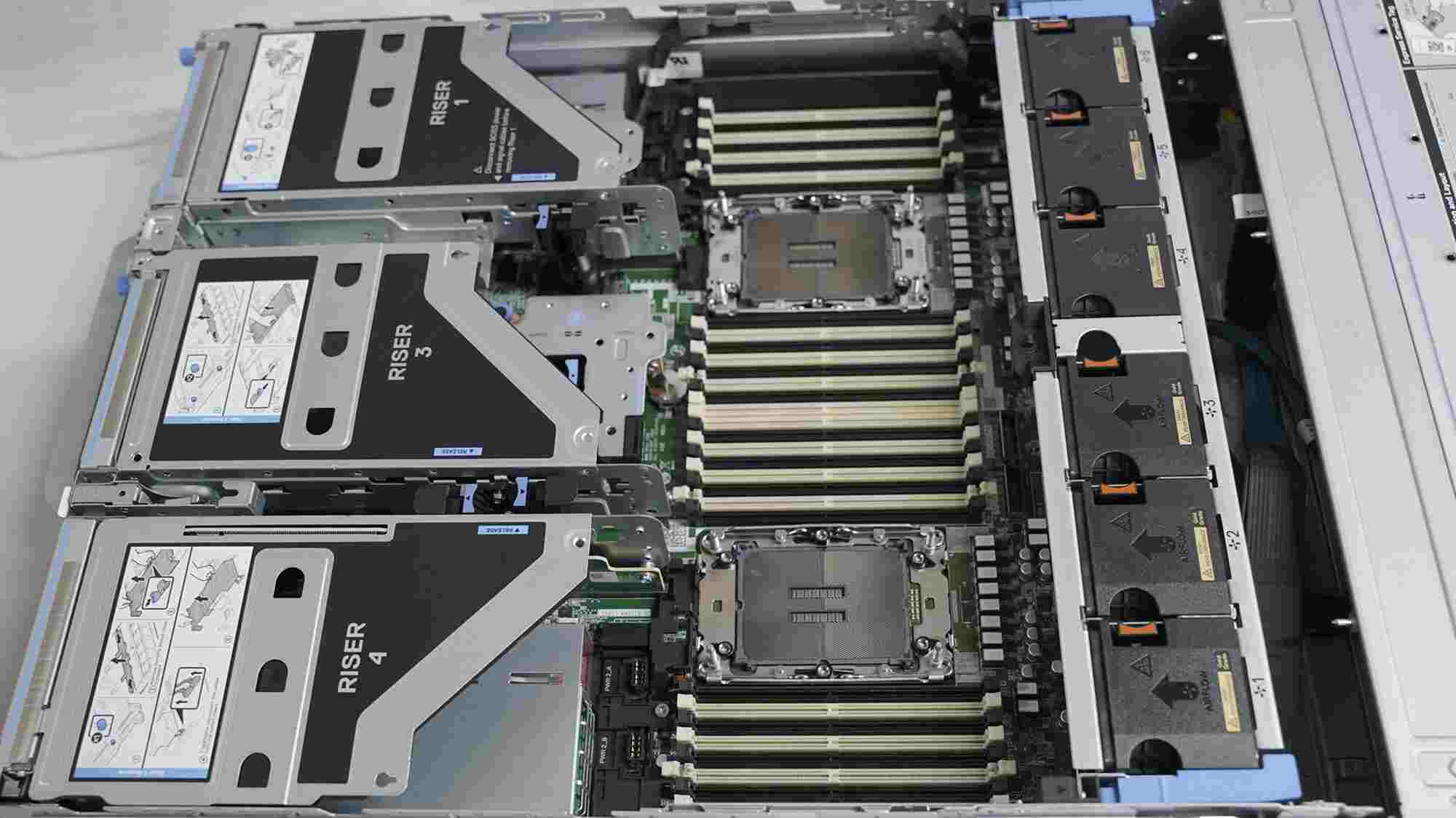
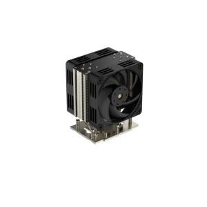
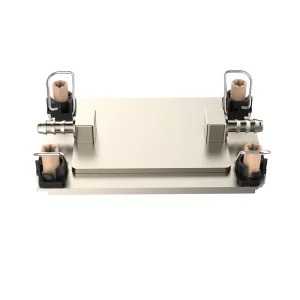
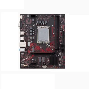
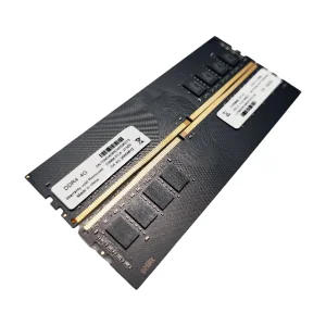
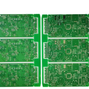
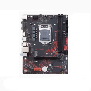
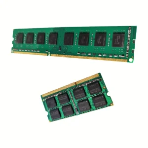
Complete selection of server heatsinks, desktop memory, and multilayer PCB units configured for SMT assembly processes in Sydney.
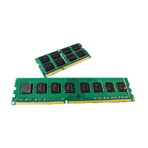
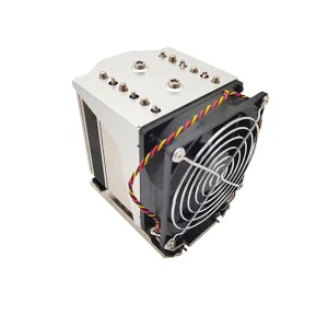
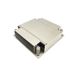
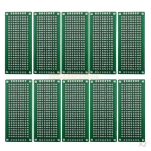
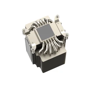
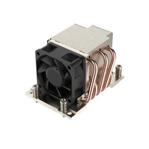
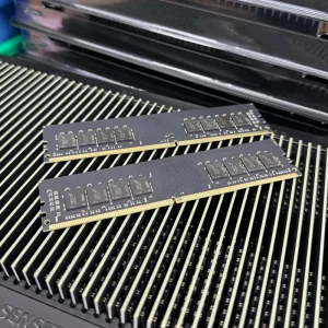

Keeping track of high-precision technological shifts that define modern electronics assembly yield rates globally.
Modern electronics require ultra-narrow aperture gaps down to 20-30 microns. Fiber Laser technology has replaced standard CO2 and older Nd:YAG lasers, drastically reducing heat-affected zones (HAZ) and thermal distortion during SMT foil fabrication. This creates smooth-walled apertures that improve transfer efficiency by up to 35%.
For high-volume high-mix SMT setups, Electroformed (E-formed) nickel stencils are used in high-end projects. However, advanced laser-cut steel stencils, combined with post-cutting chemical etching or electropolishing processes, provide matching stencil wall smoothness at a fraction of the cost, making them the preferred budget-yield compromise globally.
With complex multi-component boards where large connectors sit next to tiny 0.4mm pitch CSPs, single-thickness foils fall short. Global SMT trends rely on Step-Up (thicker local regions for large connectors) and Step-Down (thinner regions for fine pitch components) laser stencils, which we manufacture via precision chemical milling or dual-foil laser welding processes.
Navigating Australian electrical manufacturing requirements requires compliance with local and international quality and eco-directives. Our stencils and manufacturing partners strictly respect RoHS (Restriction of Hazardous Substances), ensuring that lead-free solder paste applications run on lead-free stencils and raw materials.
Furthermore, Velmix Technology is fully aligned with ISO9001:2015 quality management systems. Each custom stencil undergoes automated optical inspection (AOI) to verify aperture alignment, dimensional geometry, and frame tension before being securely packed inside protective, heavy-duty wooden crates suitable for long-distance air freight. This guarantees that your stencil arrives flat, tensioned, and ready to slot into your printer system (e.g., DEK, MPM, or Yamaha screen printers).
Answering the most critical engineering and logistic questions for Sydney electronics manufacturing projects.
Typically, custom stencil fabrication takes 24 hours from the approval of the DFM check. Shipping via priority air service to Sydney airport (SYD) takes approximately 2-4 business days. The total delivery time is generally between 3 and 5 business days, making it comparable to, and often faster than, local fabrication queues.
The area ratio is defined as the area of the aperture opening divided by the surface area of the aperture walls. For a rectangular aperture of width (W) and length (L) on a stencil foil of thickness (T), the formula is: Area Ratio = (W x L) / (2 x (W + L) x T). Per IPC-7525 standard, this ratio should be greater than 0.66 for consistent solder paste release.
Chemical etching creates a double-sided profile that narrows in the middle (hourglass shape), resulting in poor paste release on components smaller than 0.5mm pitch. In contrast, fiber laser cutting cuts directly through the metal foil, creating clean, vertical walls with a slight natural taper, significantly improving paste deposition accuracy.
We accept standard PCB CAD output formats, including Gerber RS-274X, Gerber X2, ODB++, and DXF/DWG. For stencil fabrication, we generally require the Solder Paste layer (typically top/bottom paste layers), copper layers (to verify component alignment pads), and the board outline layer.
Yes, we offer premium hydrophobic and oleophobic nano-coatings. This ultra-thin, wipe-on or vacuum-deposited chemical layer prevents solder paste from sticking to the stencil walls and underside, ensuring better print definition and reducing SMT printer paper roll and solvent cleaning cycles.
Partner with Velmix Technology Co., Ltd. for rapid SMT stencil fabrication, professional DFM analysis, and highly reliable PCB thermal management solutions. Get custom quotes in under 24 hours.
Send Inquiry Now Velmix