High-precision infrastructure components optimizing paste printing and thermal cooling efficiency across Southeast Asian assembly houses.
Malaysia has long been established as a global hub for electronics manufacturing services (EMS), outsourcing semiconductor assembly and test (OSAT) units, and automotive electronics. The industrial zones of Penang (the Silicon Valley of the East), Johor, and the Klang Valley require extremely precise SMT tooling to cater to modern micro-BGA components and 01005 passives.
With the massive rise of smart manufacturing, automotive safety sensors, IoT devices, and 5G networking nodes in Malaysia, the margin for error in solder paste printing is zero. This is where high-quality laser-cut stencils step in to ensure exact volume deposition, avoiding solder bridges, voiding, or incomplete connections on high-density interconnect (HDI) PCBs.
By sourcing advanced stencils designed with specialized apertures (such as micro-modifications and step-down pockets), manufacturers across Southeast Asia are achieving lower defect rates, boosting line yields, and lowering production costs.
Serving world-class OSAT networks and local EMS hubs with quick-turn laser stencil designs to expedite hardware prototype validation.
Delivering stencils compliant with strict ISO9001 and IPC-7525 guidelines, required for crucial safety modules and ADAS system designs.
Exploring the structural modifications required to print solder paste consistently onto high-complexity PCBA designs.
Hydrophobic and flux-phobic nano-coatings repel solder paste residues, reducing stencil cleaning frequency up to 70% and ensuring consistent volume transfer for micro-apertures down to 0.4mm pitch.
Enables localized solder paste thickness control. Thicker areas (step-up) deliver extra volume for large connector leads, while thinner areas (step-down) prevent bridges on fine-pitch QFN and BGA footprints.
Utilizing advanced chemical/electro polishing steps post-laser-cutting to smooth the internal walls of the apertures, eliminating microscopic burrs that cause paste release sticking issues.
How cross-border industrial integration between Shenzhen and Malaysia guarantees faster lead times, massive cost efficiency, and premium quality standards.
Shenzhen's manufacturing hub functions as the global epicenter for electronics prototyping and high-volume assemblies. Leveraging our location, **Velmix Technology Co., Ltd.** connects advanced material sciences with streamlined supply lines. For Malaysian clients, this means access to high-grade imported German stainless steel foils, state-of-the-art multi-beam laser cutting machines, and prompt air shipping logistics that land products directly in Kuala Lumpur or Penang in 2 to 3 days.
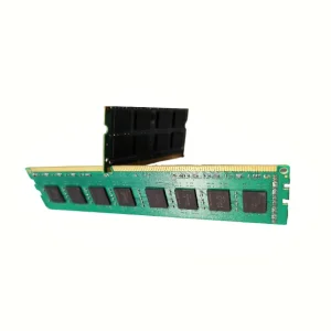
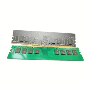
Our deep industry integration is built on 15 years of technical expertise. We not only manufacture custom memory modules and PCBA prototypes, but also guide engineers to match their aperture files (Gerbers) to ideal aspect/area ratios conforming strictly to the IPC-7525B standard, mitigating paste printing defects before manufacturing even starts.
Our dedicated engineering department checks and scales your Gerber data design to compensate for paste shrinkage and pad layouts.
All stencils are shipped in damage-proof plywood crates or reinforced cardboard frames directly utilizing DHL/FedEx or regional premium air cargo lanes.
A professional high-performance electronics and packaging solutions manufacturer based in Shenzhen, China.
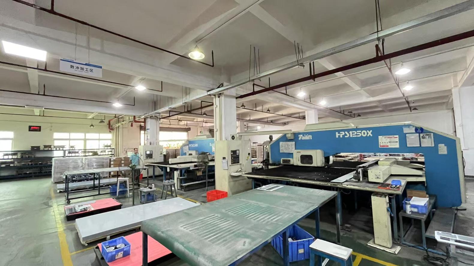

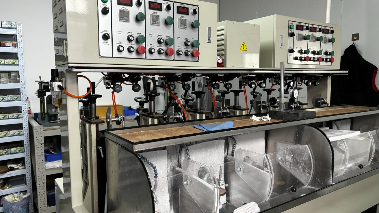
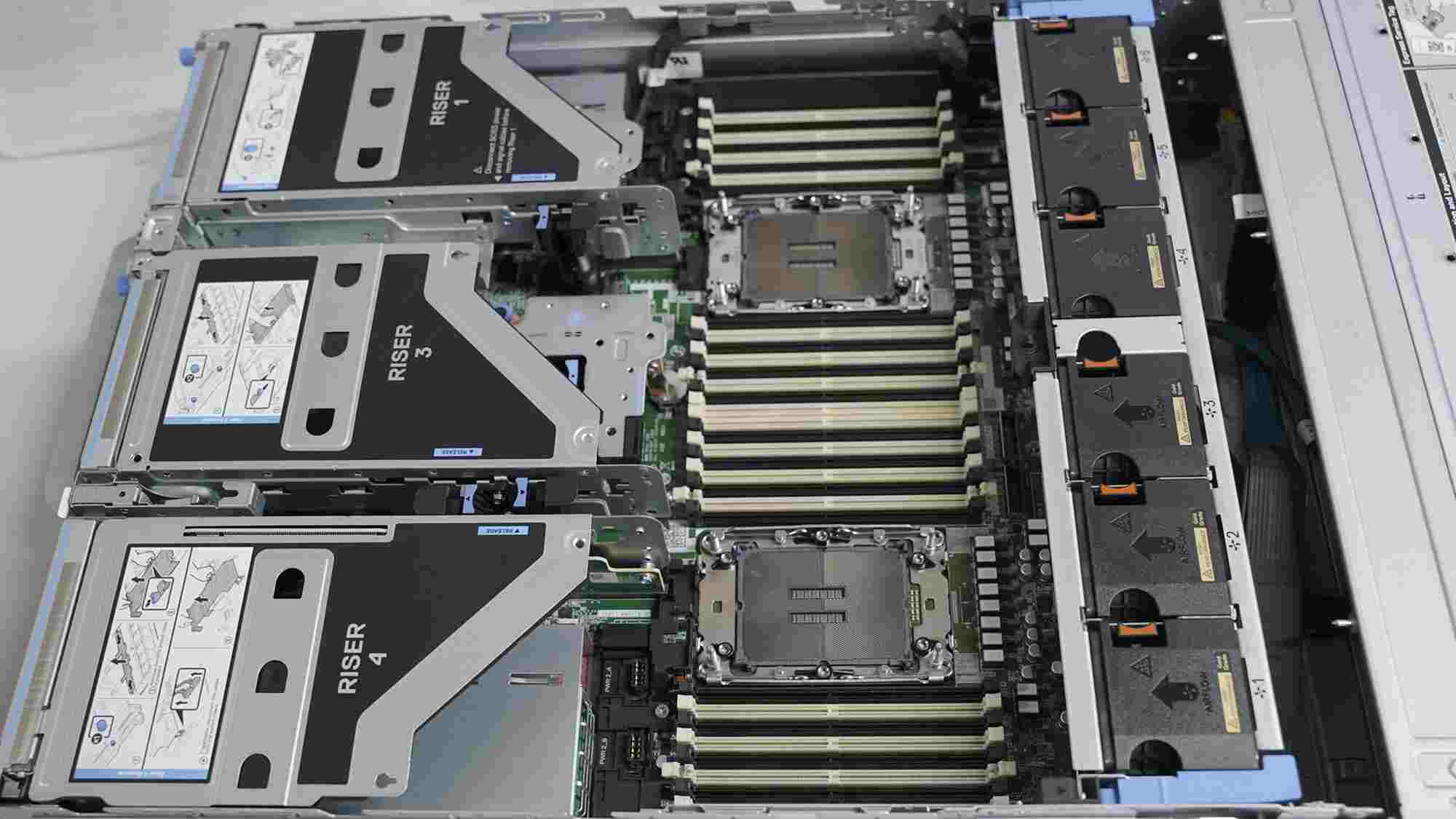
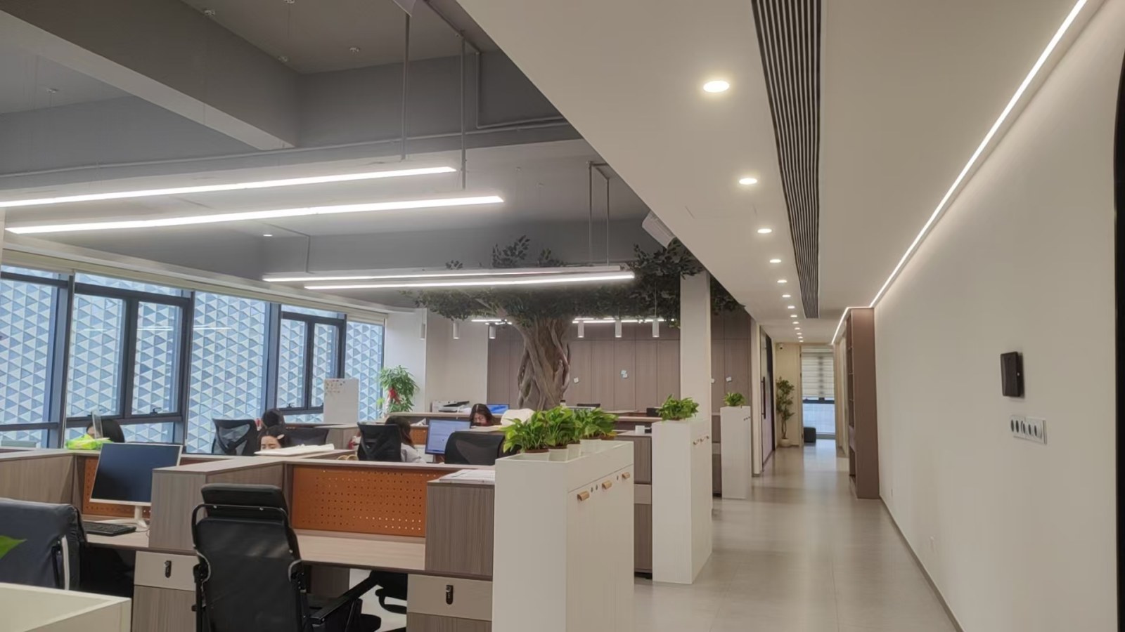
| Specification Item | Velmix Company Profile & Quality Metrics |
|---|---|
| Company Name | Velmix Technology Co., Ltd. |
| Established | 2017 |
| Facility Area | 368㎡ |
| Annual Export Revenue | USD 18.6 Million |
| Export Experience | 8 Years |
| Industry Experience | 15 Years |
| Quality Control | 100% Full Inspection Before Shipment |
| Product Inspection Methods | Signal Integrity Test, Burn-in Test, Compatibility Test, Functional Test & Random Sampling |
| QC Staff | 56 Employees |
| Business Type | Manufacturer & Exporter |
| Main Markets | North America, Europe, Southeast Asia, Middle East & South America |
| Supply Chain Partners | 986+ |
| Main Customer Types | Brand Owners, OEM Manufacturers, System Integrators, Distributors & Wholesalers |
| R&D Capability | Independent Product Design, PCB Development & Firmware Optimization |
| Customization Options | OEM, ODM, Private Label, Customized Capacity, Heat Spreader, PCB Color & Packaging |
| New Products Launched Last Year | 138 Models |
| R&D Engineers | 84 Engineers |
Driven by innovation, precision manufacturing, and customer-oriented service, Velmix continues to expand its portfolio of DDR5 memory products while helping global partners build faster, more reliable, and more efficient computing systems. We are dedicated to becoming a trusted long-term supplier of premium memory solutions for customers worldwide.
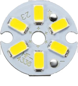
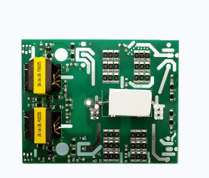
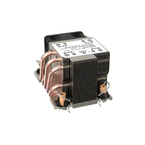
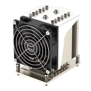
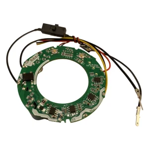
Explore our wide array of customizable PCB components, server computing accessories, and driver boards optimized for Southeast Asia industrial infrastructures.
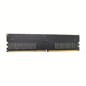
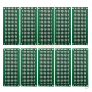
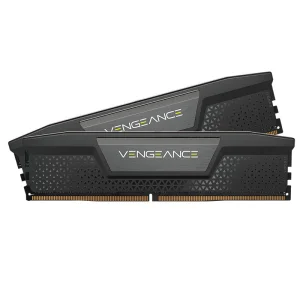
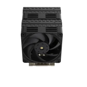
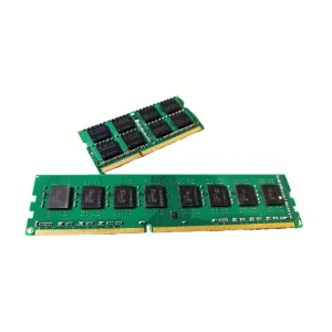
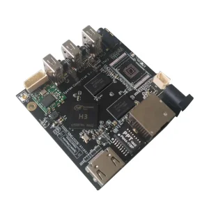
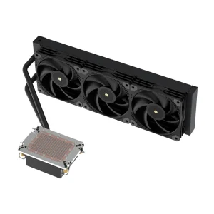
Determining stencil thickness and aperture size reduction is critical to optimizing solder paste transfer ratio. As a general rule of thumb, our design engineers refer to the standard calculation metrics to evaluate layout feasibility:
By employing our fiber-laser cutting machines operating at 20,000Hz pulse frequency, the dimensional variance is controlled within ±2 micrometers. This extreme precision ensures that multi-million point PCB boards print without single-bridge or skipped printing errors.
Unsure whether to choose 120-micron or 150-micron stencil foils for your fine-pitch BGA or CSP components? Send your Gerber files to our R&D engineering desk, and we will perform a complimentary SMT manufacturability check (DFM analysis) within 3 hours.
Clear, authoritative technical answers addressing common procurement questions regarding laser stencils and global shipping logistics.
Simplify your supply chain logistics. Send your Gerber and fabrication details to get a customized, highly competitive OEM production proposal within a few hours.
 Velmix