Optimized layout solutions for high-mix, low-volume and mass production runs across Canada's engineering and aerospace corridors.
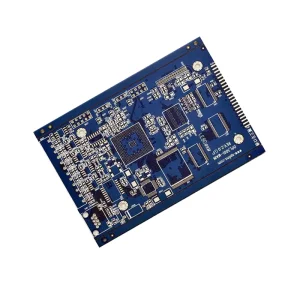
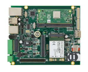
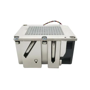
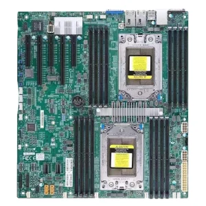
Canada's advanced manufacturing landscape is undergoing a significant transformation. Driven by high-growth sectors such as aerospace in Quebec, automotive innovation in Southern Ontario's tech corridor, clean technology hubs in British Columbia, and biomedical systems in Montreal, the need for localized precision engineering has never been higher. SMT (Surface Mount Technology) assembly is the cornerstone of these high-tech developments. Within this ecosystem, laser stencils serve as the critical entry point to successful solder paste deposition, directly dictating assembly yield and overall product reliability.
In major hubs like the Toronto-Waterloo tech corridor and Ottawa's telecommunications cluster, prototyping cycles are rapid. Local PCB assembly operations require extreme accuracy. High-precision laser-cut stencils are necessary to achieve optimal print quality for miniaturized components, including 0201, 01005, and fine-pitch BGA (Ball Grid Array) components. However, sourcing stencils locally in Canada often encounters constraints regarding custom engineering support, advanced nano-coating accessibility, and cost-efficiency for multi-level step stencils.
As a specialized laser stencil and PCBA material manufacturer, we bridge this gap by delivering premium-grade laser-cut stencils and thermal/memory system solutions directly to the Canadian electronics assembly market. By utilizing state-of-the-art German laser systems and premium-grade fine-grain stainless steel, we ensure that Canadian OEMs, EMS (Electronic Manufacturing Services) providers, and research laboratories receive hardware that matches strict IPC standards.
For Canadian procurement managers, balancing cost, lead time, and precision is critical. Sourcing from our manufacturing facility in Shenzhen, China, provides distinct commercial and technical advantages:
The SMT industry is moving away from basic chemical etching and standard laser cutting toward complex multi-level stencil architectures. As electronics shrink and double-sided boards integrate both high-power components and micro-footprint processors, standard uniform stencils cannot always deposit the correct amount of paste for every footprint.
Step Stencils (Step-Up & Step-Down): This design variation modifies local stencil thickness. For example, a base thickness of 120μm can be locally reduced to 100μm (step-down) to prevent bridging on a fine-pitch QFN component, or increased to 150μm (step-up) to provide sufficient solder volume for large connector leads or power semiconductor components.
Electroformed & Nano-Coated Stencils: The introduction of nano-coatings has altered high-volume SMT lines. By applying a molecular-thin coating, the stencil repels flux oils and solder balls. This prevents paste buildup, which is particularly beneficial for high-density components on modern communication equipment and automotive control systems.
Our precision-made stencils and electronics hardware are optimized for specific industrial and commercial environments across Canada:
Velmix Technology Co., Ltd. is a professional DDR5 memory manufacturer based in Shenzhen, China, specializing in the research, development, production, and global distribution of high-performance DRAM memory solutions. Since its establishment in 2017, Velmix has been committed to delivering reliable, high-speed memory products for consumer electronics, industrial applications, gaming systems, servers, and embedded computing.
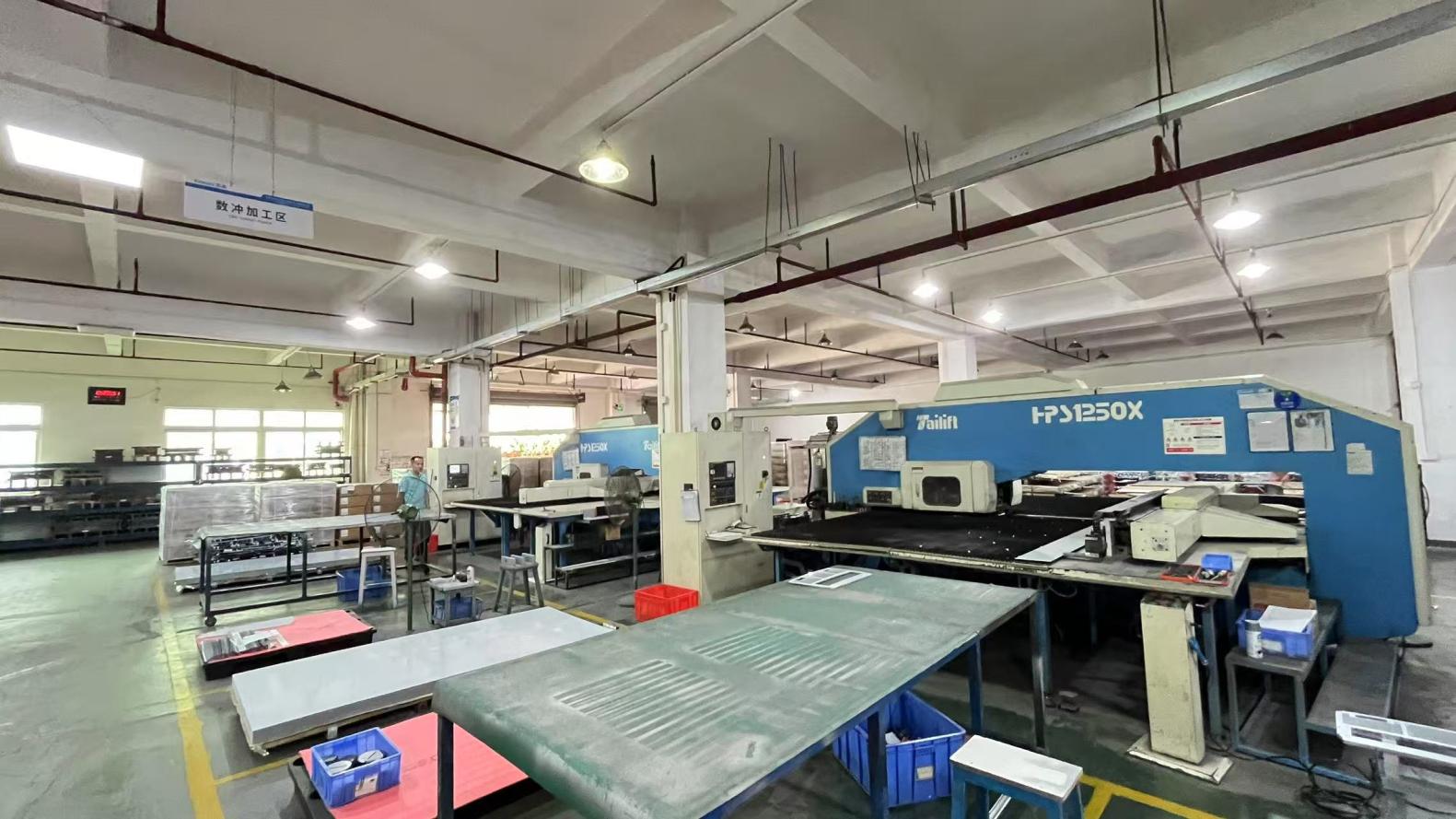
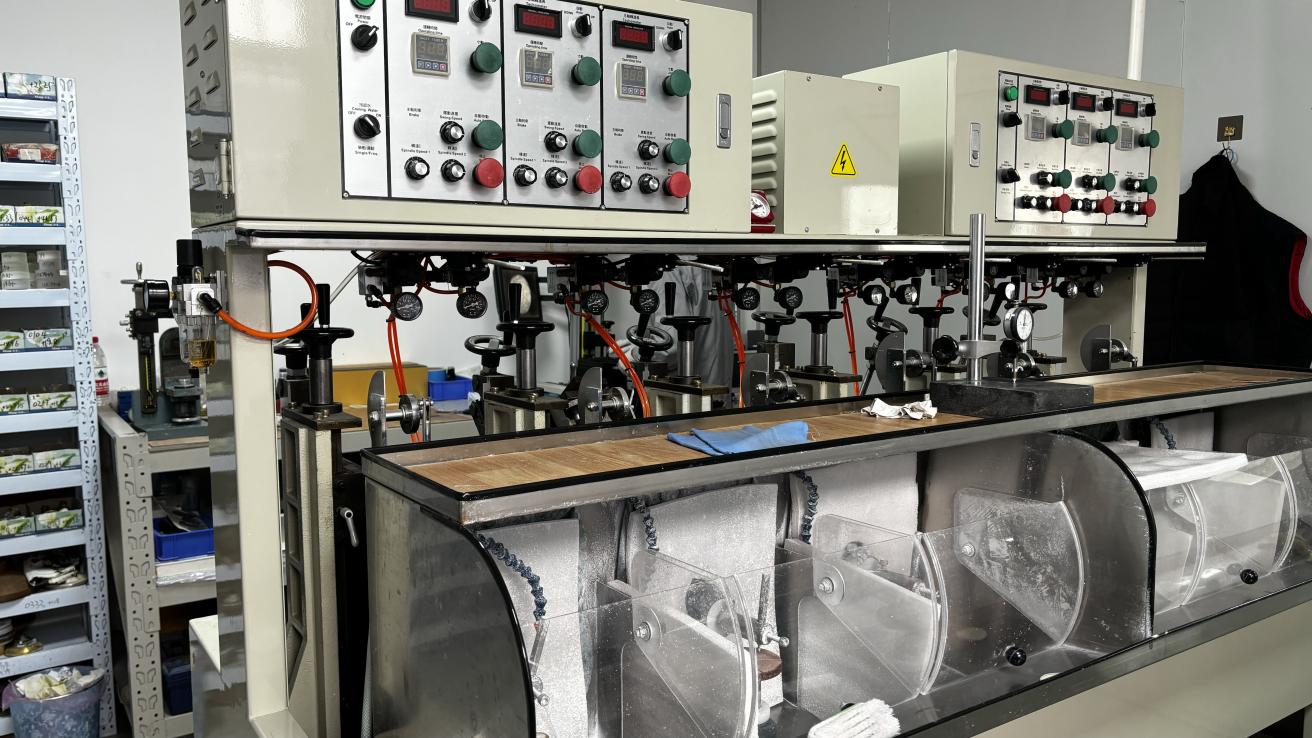
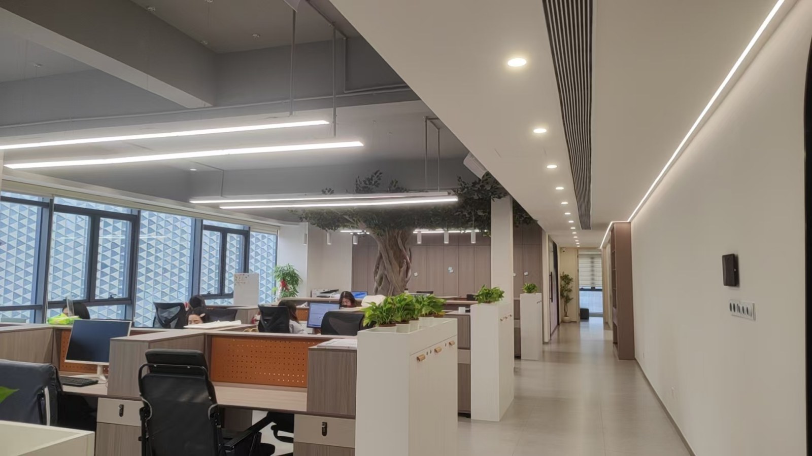
Operating from a modern manufacturing facility covering 368㎡, we combine advanced production technologies with strict quality management to ensure every memory module meets international performance and reliability standards. Our experienced engineering team continuously develops innovative DDR5 memory solutions to meet the evolving demands of AI computing, edge devices, cloud infrastructure, and next-generation computing platforms.
Today, Velmix serves customers in more than 40 countries and regions, offering flexible OEM and ODM manufacturing services for global brands, distributors, system integrators, and industrial equipment manufacturers. By focusing on product consistency, fast delivery, and technical innovation, we have built long-term partnerships across Europe, North America, Southeast Asia, and the Middle East.
| Item | Information |
|---|---|
| Company Name | Velmix Technology Co., Ltd. |
| Established | 2017 |
| Facility Area | 368㎡ |
| Annual Export Revenue | USD 18.6 Million |
| Export Experience | 8 Years |
| Industry Experience | 15 Years |
| Quality Control | 100% Full Inspection Before Shipment |
| Product Inspection Methods | Signal Integrity Test, Burn-in Test, Compatibility Test, Functional Test & Random Sampling |
| QC Staff | 56 Employees |
| Business Type | Manufacturer & Exporter |
| Main Markets | North America, Europe, Southeast Asia, Middle East & South America |
| Supply Chain Partners | 986+ |
| Main Customer Types | Brand Owners, OEM Manufacturers, System Integrators, Distributors & Wholesalers |
| R&D Capability | Independent Product Design, PCB Development & Firmware Optimization |
| Customization Options | OEM, ODM, Private Label, Customized Capacity, Heat Spreader, PCB Color & Packaging |
| New Products Launched Last Year | 138 Models |
| R&D Engineers | 84 Engineers |

Our standard production time is 24 hours from CAD design confirmation. Using express shipping services (like DHL or FedEx), delivery to major Canadian cities (such as Toronto, Montreal, Vancouver, and Ottawa) takes 2 to 4 business days.
Our engineering team checks all incoming Gerber files against standard IPC-7525 guidelines. We focus on keeping the aspect ratio greater than 1.5 and the area ratio greater than 0.66. If needed, we will propose minor aperture modifications to optimize solder paste release.
Nano-coating modifies the stencil surface to be hydrophobic and oleophobic. This treatment reduces solder paste sticking to the aperture walls, resulting in cleaner print definition and fewer cleaning cycles, which is helpful for high-density components on SMT lines.
Yes. We design and manufacture multi-level stepped stencils (thickness variations ranging from 0.08mm to 0.25mm) to accommodate different component heights and solder volume requirements on a single board.
Yes, we supply framed laser stencils (compatible with standard pneumatic systems like DEK or MPM printers) as well as frameless stencils (compatible with universal quick-change tension frames like ZelFlex or LPKF systems).
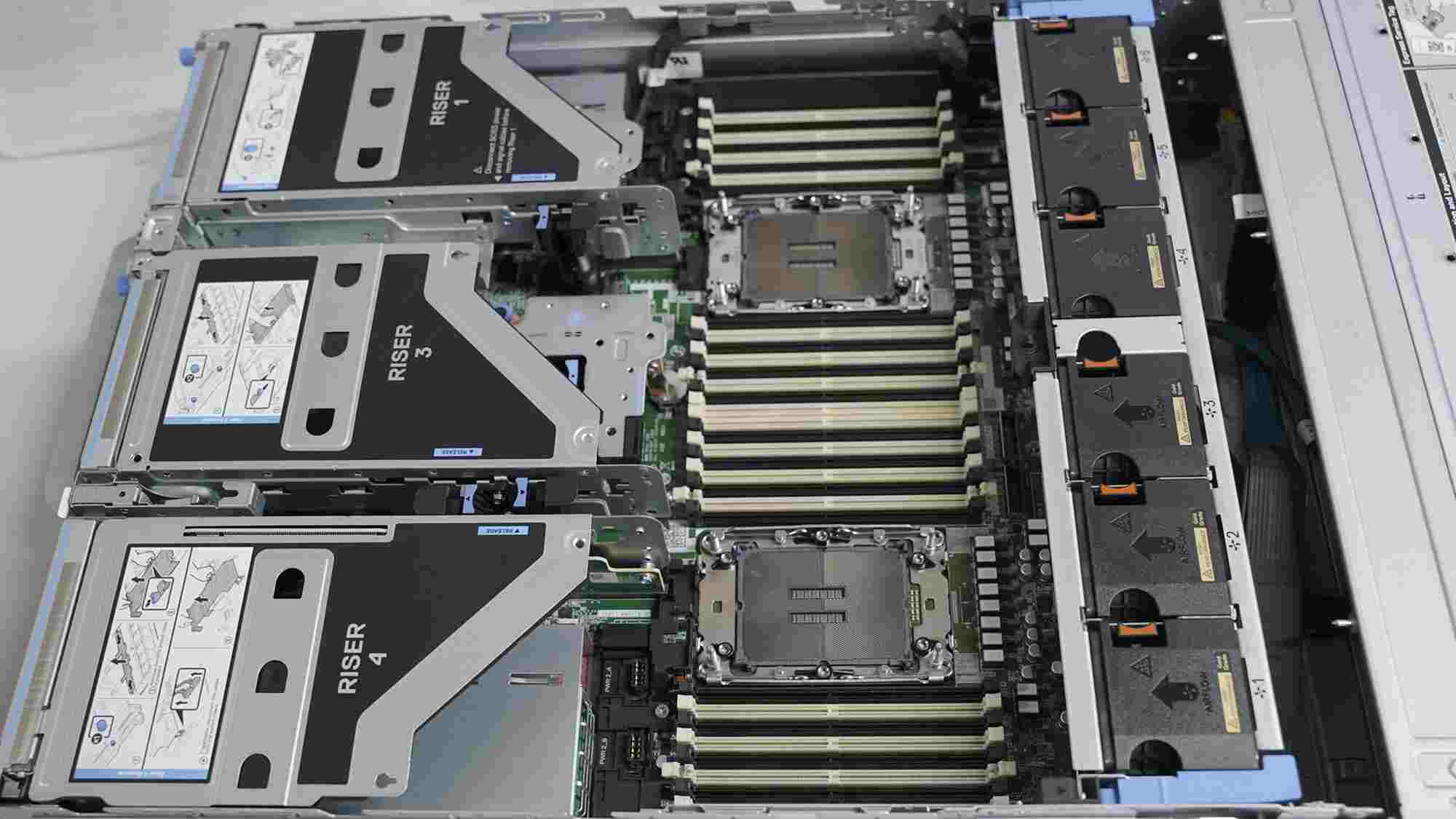
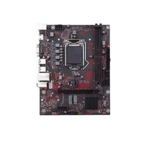
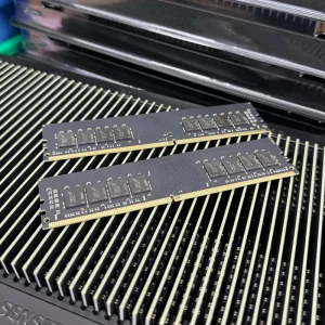
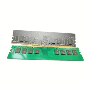
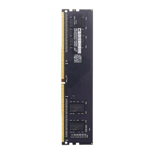
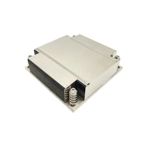
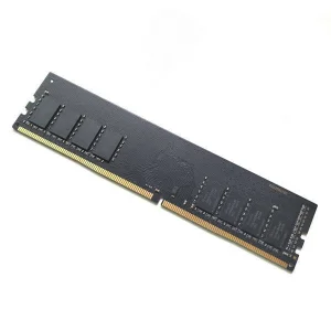
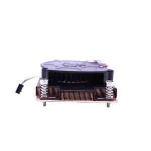
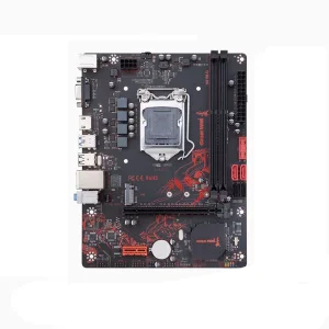
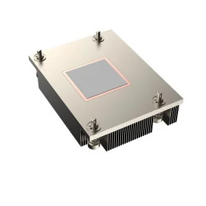
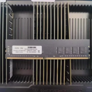
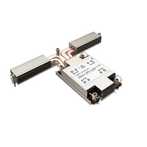
High-speed RAM modules, industrial motherboards, and server cooling solutions for advanced computer systems and industrial platforms in Canada.
 Velmix