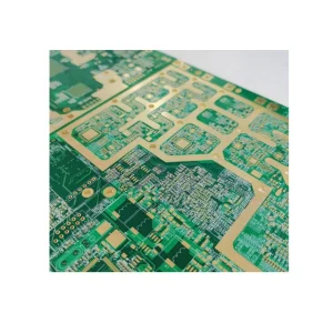
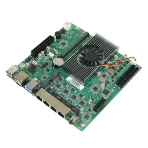
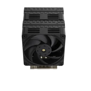
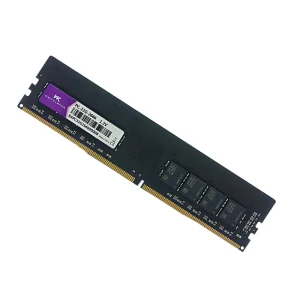
As East Africa undergoes rapid digital transformation, South Sudan is strategically upgrading its communication infrastructures, wireless backhauls, and localized industrial computing systems. In cities like Juba, Malakal, and Wau, the installation of telecommunication towers, civil aviation monitoring systems, and oil field control nodes requires advanced electronic hardware that can perform under severe atmospheric and operational conditions. High-Frequency Printed Circuit Boards (RF/Microwave PCBs) act as the physical backbone for these high-frequency applications, allowing signal transmissions above 1 GHz to execute with minimal attenuation and signal skew.
This whitepaper addresses the design paradigms, material sciences, manufacturing capabilities, and export pathways essential to delivering high-frequency PCBs and high-speed computing modules to South Sudan. Backed by the manufacturing expertise of Velmix Technology Co., Ltd., we combine state-of-the-art lamination protocols with rigorous high-speed testing (Signal Integrity, Burn-in, and Thermal Shock) to serve regional telecommunication agencies, off-grid power grids, and industrial computing infrastructures.
The performance of a High-Frequency PCB is determined by the material properties of its core laminate and prepreg layers. Standard FR-4 substrates, which are sufficient for kilohertz or low-megahertz digital circuits, experience excessive signal loss (Dissipation Factor, $D_f$) and variations in their Dielectric Constant ($D_k$) when subjected to gigahertz frequencies. This degrades signal integrity and produces localized thermal spikes.
To preserve signal fidelity in microstrip, stripline, and coplanar waveguide layouts, we employ high-frequency materials from industry-recognized manufacturers, including Rogers Corporation and Shengyi Technology:
"By combining Shengyi High-TG FR4 with Rogers 4000 series substrates under precise mixed-pressure lamination, we deliver boards that handle high power and high frequency simultaneously, ensuring reliable operation for telecom backhauls across East Africa."
The operating environment in South Sudan presents specific engineering challenges, including ambient daytime temperatures exceeding 40°C, airborne dust, and remote electrical grids prone to voltage fluctuations. The implementation of high-frequency PCBs and industrial computing units must address these local environmental conditions.
Modern mobile communication in South Sudan relies on microwave links to connect Juba with outlying regional capitals. Tower-mounted transceiver modules require multi-channel RF power amplifiers constructed on Rogers PCBs to process LTE and upcoming 5G signals. These high-frequency systems must operate continuously in outdoor enclosures without failing due to thermal build-up.
With limited access to centralized power grids, communities and industrial facilities in South Sudan rely heavily on solar installations. High-frequency power conversion stages in microgrid inverters utilize high-frequency PCBs to coordinate fast-switching silicon carbide (SiC) or gallium nitride (GaN) transistors. These substrates require high thermal conductivity, often integrated with aluminum backings, to dissipate heat effectively.
In the oil extraction zones of the Upper Nile and Unity States, downhole sensors, directional drilling telemetry, and pipeline flow meters require robust controllers. High-frequency boards designed with high glass transition temperatures (High-TG) prevent delamination and solder joint cracking caused by mechanical vibration and elevated underground temperatures.
The global demand for high-frequency PCBs is driven by the expansion of 5G, autonomous transportation, IoT, and high-performance computing (AI/ML data centers). For South Sudan, procuring these components requires importing from advanced manufacturing hubs like Shenzhen, China, via sea routes through the Port of Mombasa (Kenya) or Port Sudan, followed by land transport corridors, or via air freight into Juba International Airport.
To manage this supply chain efficiently, Velmix Technology Co., Ltd. coordinates with global freight forwarding partners to ensure import compliance, customs clearance, and secure transit. Our 8 years of export experience help us assist East African system integrators in managing the logistics of high-frequency laminates, specialized server motherboards, and memory modules.
As communication frequencies move from the sub-6 GHz spectrum into millimeter-wave (mmWave) ranges, PCB manufacturing must adapt to tighter design tolerances. Our technology roadmap focuses on four key areas:
Established in 2017, Velmix Technology Co., Ltd. specializes in high-performance DRAM memory solutions and advanced PCB engineering. Our manufacturing facility in Shenzhen, China, utilizes automated surface mount technology (SMT) lines and reflow ovens to produce reliable electronic assemblies.
Our quality control framework spans the entire fabrication process. Every high-frequency PCB and memory module undergoes a strict testing regimen, including automated optical inspection (AOI), in-circuit testing, thermal cycle burn-in, and signal integrity evaluation. This testing process ensures that all components delivered to our clients in East Africa meet international performance standards.
| Operational Parameter | Technical Capability / Company Fact |
|---|---|
| Company Name | Velmix Technology Co., Ltd. |
| Established Year | 2017 |
| Facility Area | 368㎡ (Highly automated SMT and precision inspection lab) |
| Annual Export Revenue | USD 18.6 Million |
| Export Experience | 8 Years |
| Industry Experience | 15 Years |
| Quality Assurance Protocol | 100% Full Inspection Before Shipment |
| Inspection Methodology | Signal Integrity Test, Burn-in Test, Compatibility Test, Functional Test & Random Sampling |
| Quality Control Staff | 56 Dedicated QC Inspectors & Technicians |
| R&D Engineers | 84 Engineers (Specializing in High-Speed PCB Layout & Signal Integrity) |
| Key Production Categories | RF PCBs, Multi-layer FR4/Rogers Hybrid PCBs, DDR4/DDR5 Memory, Embedded Motherboards |
| Customization Scope | OEM, ODM, Private Label, Customized Capacity, Heat Spreader, PCB Color & Packaging |
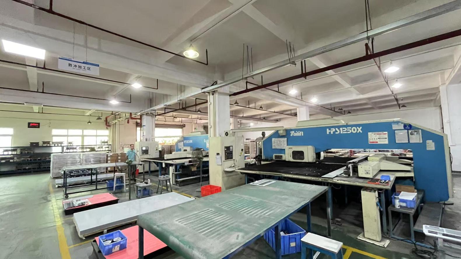
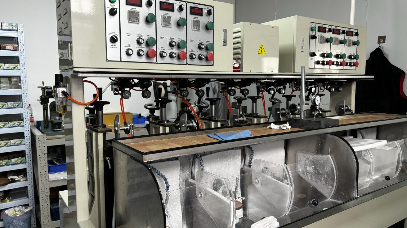
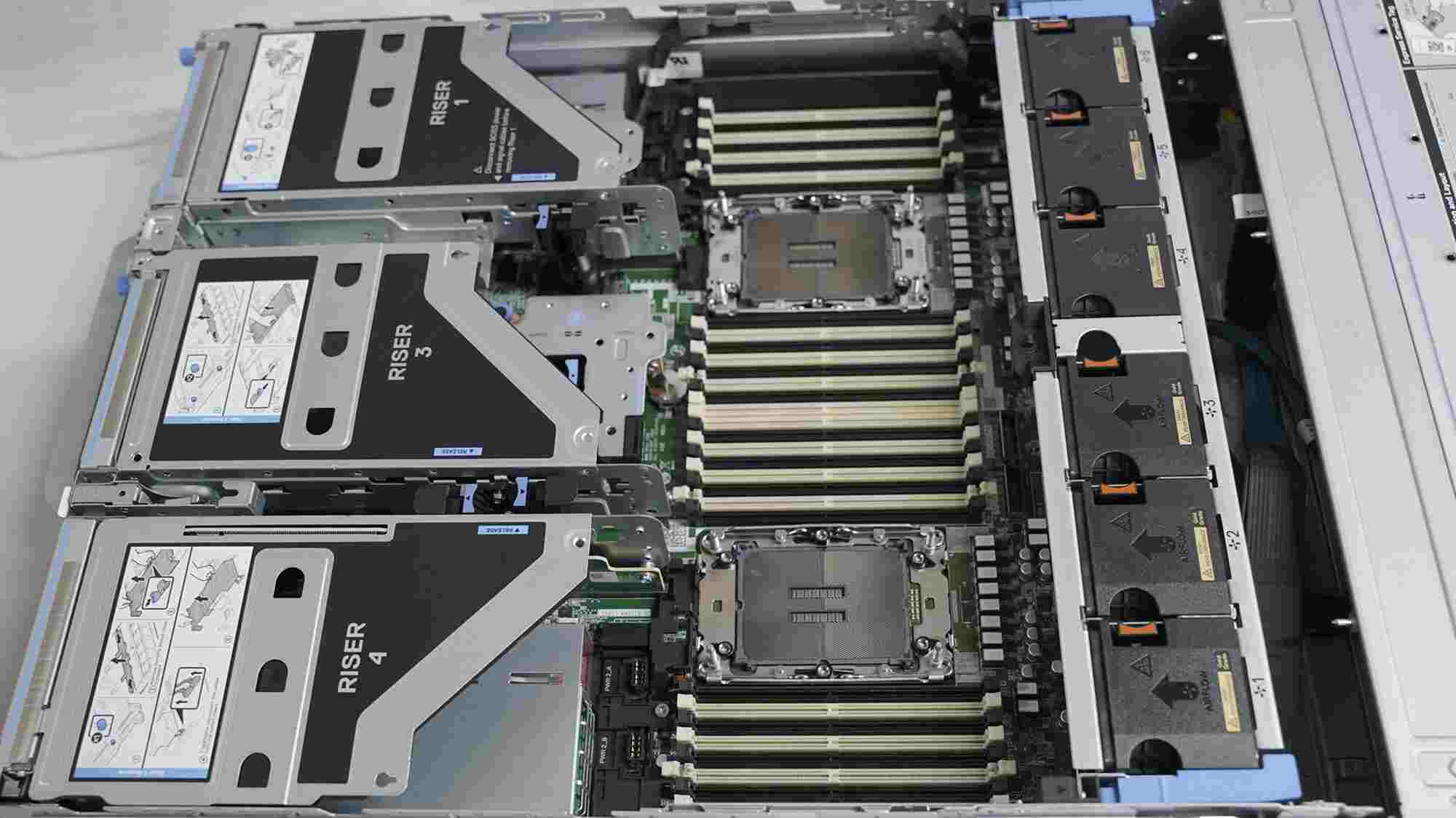
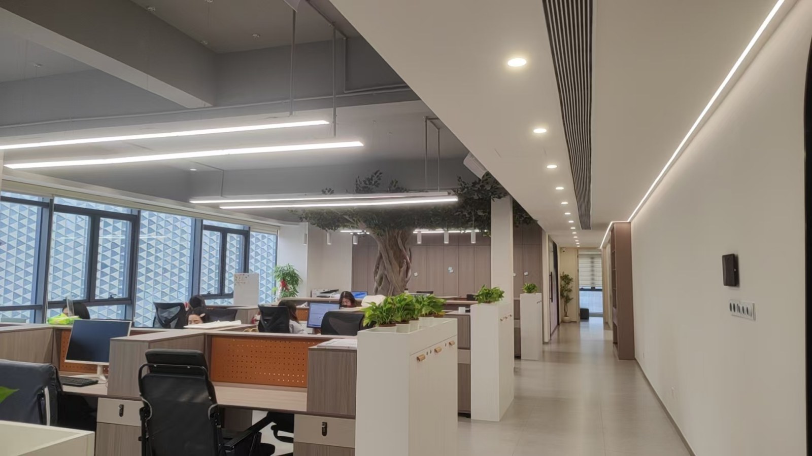
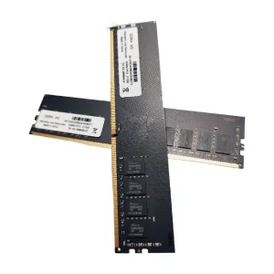
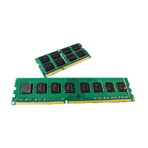
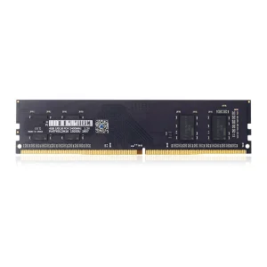
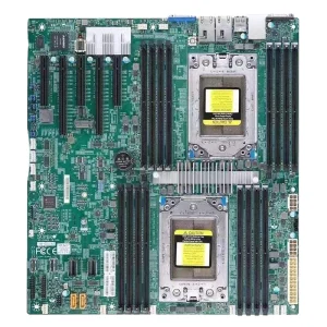
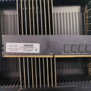
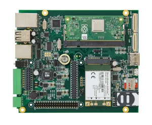
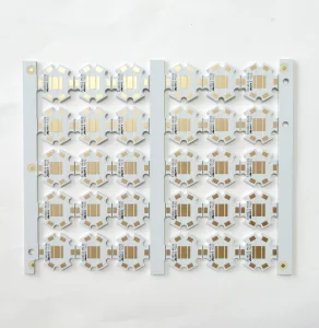
The following images document our manufacturing processes, including automated chip placement, high-precision optical alignment, thermal stress chambers, and multi-layer PCB pressing facilities.


Need expert engineering advice on high-frequency stackups, material selection, or volume quoting?
Send Inquiry Now Velmix