Explore our core collection of advanced memory modules, motherboard solutions, thermal heatsinks, and double-sided PCB production machines designed for complex computing and power configurations.
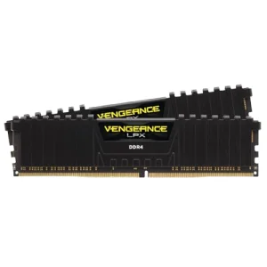
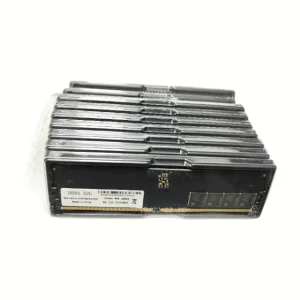
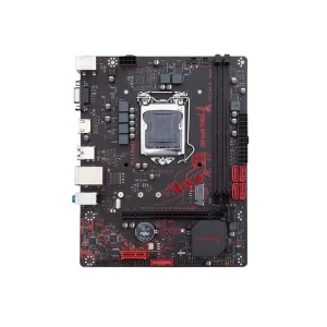
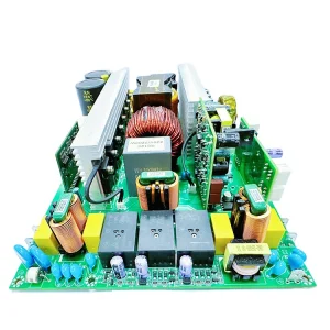
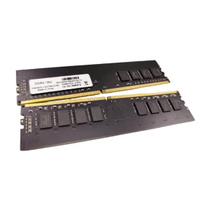
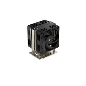

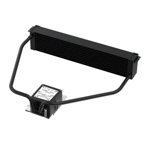
Velmix Technology Co., Ltd. is a professional technological innovator and hardware manufacturer based in Shenzhen, China, specializing in the research, development, high-precision assembly, and global distribution of high-performance DRAM memory solutions and advanced printed circuit board integrations. Since our establishment in 2017, Velmix has committed to delivering reliable, high-density, and high-speed memory systems alongside complex PCB layouts for consumer electronics, industrial automation, high-frequency gaming platforms, server environments, and embedded computing systems.
Operating from a modern, state-of-the-art manufacturing facility covering 368㎡ in the electronic epicenter of the world, we fuse cutting-edge production methodologies with an airtight quality management framework. By incorporating automated SMT mounting, high-precision AOI inspection, and custom design pipelines, we ensure that every dual-layer printed circuit board and memory module satisfies rigorous global benchmark expectations. Our highly experienced engineering team continuously optimizes impedance configurations, substrate thermal dissipation, and signal integrity to stay ahead of the escalating performance demands within artificial intelligence (AI) processing, edge devices, high-bandwidth storage networks, and cloud infrastructures.
Today, Velmix proudly serves enterprise consumers, system integrators, and OEM/ODM distributors across more than 40 countries. By cultivating robust upstream alliances and implementing 100% full-process testing, we guarantee product delivery speed, technical support accessibility, and manufacturing consistency. Whether you are looking for standardized double-sided PCB fabrications or complex PCBA system layouts, our design ecosystem provides the agility and engineering depth necessary to keep your products competitive.
To provide complete clarity on our manufacturing scale, operational experience, and quality benchmarks, the table below represents our core capabilities as a leading developer and exporter of high-grade memory products and circuit boards:
| Performance / Operational Indicator | Verified Capabilities & Standards |
|---|---|
| Company Name | Velmix Technology Co., Ltd. |
| Established | 2017 |
| Facility Area | 368㎡ (Highly optimized cleanrooms for SMT and inspection) |
| Annual Export Revenue | USD 18.6 Million |
| Export Experience | 8 Years |
| Industry Experience | 15 Years |
| Quality Control Protocol | 100% Full Inspection Before Dispatch (Zero-Tolerance Policy) |
| Product Inspection Methods | Signal Integrity Test, Burn-in Thermal Test, OS-Level Compatibility, Functional Diagnostics & Random Sampling Analysis |
| Quality Control Staff | 56 Certified Employees |
| Business Model | Manufacturer, Design Integrator & Direct Exporter |
| Main Markets Served | North America, Western/Northern Europe, Southeast Asia, Middle East, and South America |
| Supply Chain Partners | 986+ Certified Material and Semiconductor Vendors |
| Main Customer Portfolios | International Brands, OEM Manufacturers, Global System Integrators, Tier-1 Distributors & Wholesalers |
| R&D Capability | Independent Structural Product Design, Multi-Layer PCB Engineering & Custom Firmware Optimization |
| Customization Options (OEM/ODM) | Private Labels, Specific PCB Material Selection, Custom Heat Sink Integration, Custom Solder Mask Colors, Specific Chip Sourcing |
| New Products Launched (Last Fiscal Year) | 138 Models |
| R&D Engineers | 84 Engineers (Specialized in RF, High-Speed Digital Logic, and Thermal Simulation) |
Double-sided printed circuit boards, also known as dual-layer PCBs, represent the foundation of modern digital electronics. By incorporating circuitry on both sides of a single insulating substrate sheet, they provide a major leap in component density and design complexity compared to basic single-layer boards. For engineers, procurement teams, and system designers, selecting a qualified double-sided circuit boards manufacturer & supplier requires an appreciation of the structural physics and material options behind these components.
At the center of any double-sided board is the dielectric substrate, most commonly FR4 (Flame Retardant 4, a woven fiberglass cloth impregnated with epoxy resin). This core is clad on both sides with thin layers of highly purified copper, typically measured in ounces per square foot (e.g., 0.5 oz, 1.0 oz, or 2.0 oz). The electrical connections between the top and bottom copper tracks are established via Plated Through-Holes (PTH). The interior walls of these drilled holes are electroplated with copper, creating a conductive path that enables dense signal routing and cross-layer power distribution.
Choosing the correct glass transition temperature (Tg) is essential. High-reliability applications utilize Tg 170°C or Tg 180°C FR4, preventing delamination and mechanical deformation during thermal fluctuations.
Controlled electroplating ensures uniform copper thickness inside vias. This prevents voiding, cracking, and impedance discontinuities that degrade high-frequency signals.
Surface treatments like HASL (Hot Air Solder Leveling), ENIG (Electroless Nickel Immersion Gold), and OSP (Organic Solderability Preservative) protect external copper pads from oxidation while ensuring solderability.
Double-sided circuit boards act as the workhorses for a massive array of commercial and industrial applications. In many specialized scenarios, multi-layer designs are unnecessarily expensive, making high-spec dual-layer boards the most cost-effective and physically resilient choice. Understanding where these boards excel helps procurement managers source materials that fit their exact operating conditions.
For global technology enterprises, sourcing PCBs is a strategic decision that impacts product quality, time-to-market, and total cost of ownership. The modern marketplace presents a choice between localized suppliers (who offer geographic convenience and face-to-face engineering reviews) and overseas hubs, particularly manufacturers based in China.
China's circuit board manufacturing industry is not just about lower labor costs; it is about an unmatched industrial ecosystem. Based in electronic hubs like Shenzhen, manufacturers like Velmix leverage integrated supply chains. This means raw copper clad laminates, solder mask inks, high-speed drilling machinery, automated optical inspection tools, and component packaging facilities are situated within a 50-kilometer radius.
This geographic concentration reduces production lead times to a fraction of what local western fabricators can achieve. In addition, China's PCB suppliers have invested heavily in high-performance robotics and automated SMT equipment, allowing for rapid scaling from prototype volumes to high-volume production runs. This scalability, combined with raw material access, offers global buyers a cost advantage of up to 40% without compromising technical standards.
High-reliability applications require strict adherence to international safety and quality standards. Experienced manufacturers must hold certifications such as ISO 9001:2015 for quality management, UL 796 for safety standards, and comply with RoHS and REACH regulations regarding hazardous substances. For mission-critical systems, boards are manufactured in compliance with IPC-A-600 Class 2 or Class 3 standards, guaranteeing structural reliability under harsh environmental conditions.
The electronic hardware industry is undergoing rapid changes driven by the rise of artificial intelligence, high-frequency telecommunications (5G and 6G), and internet-of-things (IoT) ecosystems. Double-sided circuit board designs are evolving to keep pace with these shifts:
For RF and radar systems, standard FR4 epoxy is replaced with specialized PTFE (Teflon) or ceramic-filled laminates (such as Rogers materials). These materials exhibit lower dielectric loss (Df), preserving signal strength at gigahertz frequencies.
To maximize space efficiency, designers are embedding passive components directly within the inner core layer of double-sided boards. This leaves the outer surfaces free for active ICs and high-density connectors.
Environmental standards are driving the adoption of halogen-free epoxy systems and bio-based resin alternatives. These eco-friendly choices reduce toxic waste during end-of-life recycling and incineration processes.
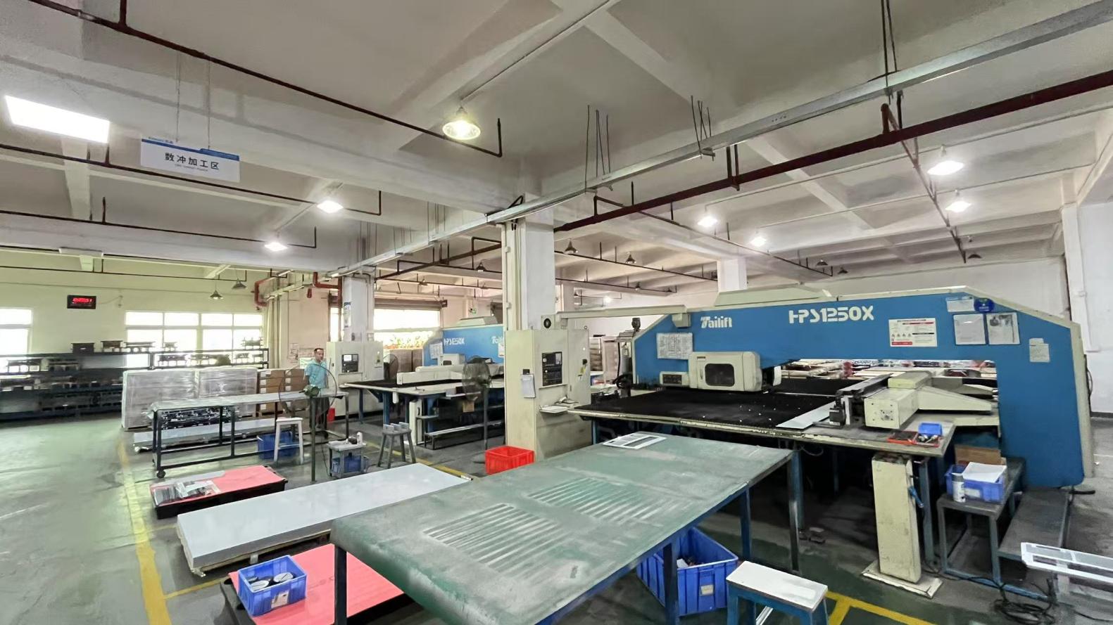
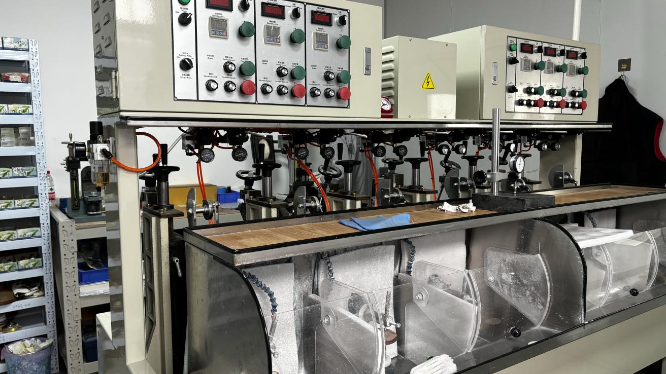
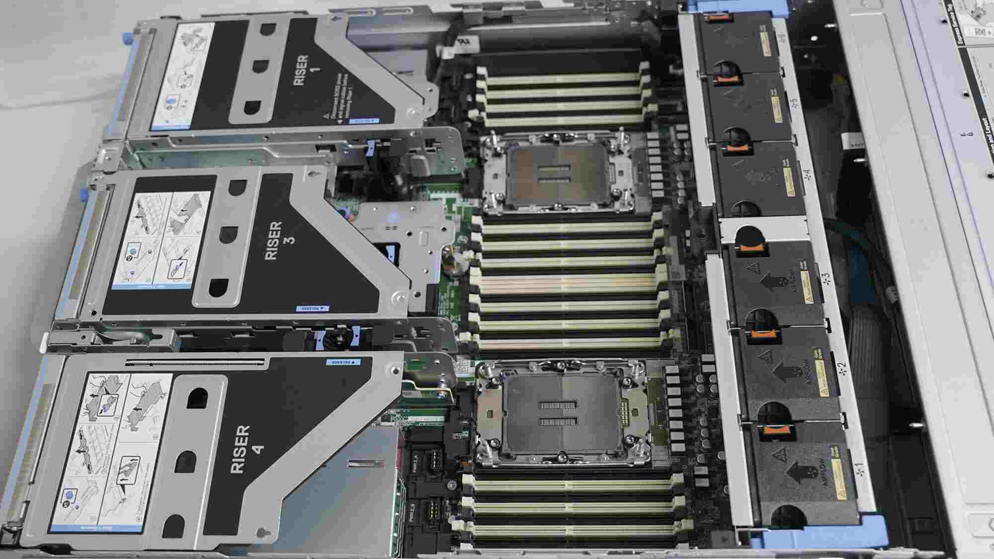
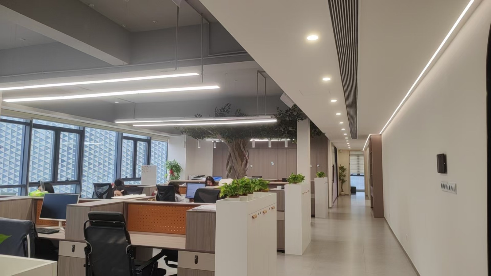
A glimpse inside our facility in Shenzhen, where high-precision engineering meets automated SMT assembly, testing, and meticulous quality control.

Find answers to the most common questions regarding double-sided circuit board design, SMT assembly, and global procurement processes.
Single-sided PCBs feature conductive copper traces on only one side of the substrate material, limiting component routing. Double-sided PCBs have copper traces on both the top and bottom surfaces, connected by Plated Through-Holes (PTH). This design allows for higher component density, smaller board sizes, and more complex circuit layouts.
The choice of surface finish depends on the application. HASL (Hot Air Solder Leveling) is cost-effective and provides good solderability, but is not ideal for fine-pitch components due to surface unevenness. ENIG (Electroless Nickel Immersion Gold) offers a flat, coplanar surface and excellent corrosion resistance, making it suitable for fine-pitch components and high-reliability systems. OSP (Organic Solderability Preservative) is eco-friendly and provides a flat surface, but has a shorter shelf life.
Copper thickness directly impacts the board's current-carrying capacity and thermal management. Standard circuit boards use 1 oz (35 microns) of copper, which is sufficient for signal lines and low-power applications. Heavy copper designs (2 oz, 3 oz, or higher) are used in power electronics, automotive systems, and solar inverters to handle larger electrical currents and dissipate heat effectively.
A reliable supplier should hold ISO 9001:2015 certifications for quality management. For safety, UL 796 recognition is standard. Compliance with RoHS and REACH regulations is necessary to meet environmental requirements, and boards should be manufactured to IPC-A-600 Class 2 (standard commercial) or Class 3 (high-reliability/aerospace/medical) standards.
Lead times vary by complexity. Standard double-sided PCB prototypes can be fabricated in 24 to 48 hours. Mass production runs usually take between 7 to 10 working days. Shipping via air express (DHL, UPS, FedEx) takes an additional 3 to 5 business days, while ocean freight for high-volume orders takes between 15 to 30 days depending on the destination port.
Velmix uses a multi-stage testing process. We perform signal integrity testing, burn-in thermal stress tests, OS-level software compatibility reviews, and automated optical inspection (AOI) to ensure all signal tracks and plated through-holes meet our zero-defect quality threshold before shipping.
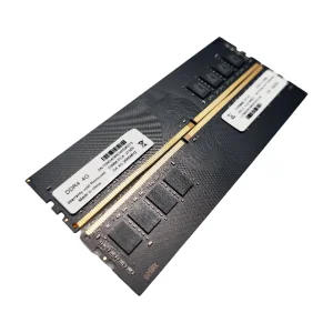
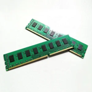
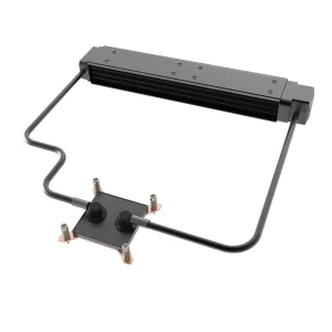
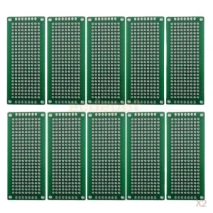
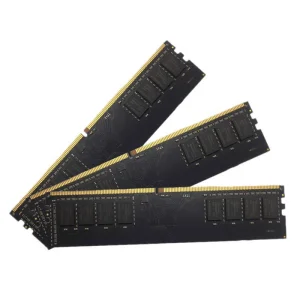
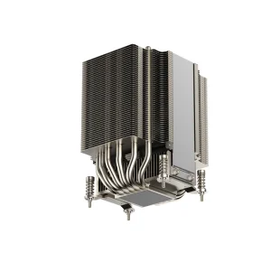
Browse the rest of our product lineup, including multi-capacity DDR4/DDR5 system memory, server cooling systems, and specialized double-sided circuit substrates.
 Velmix