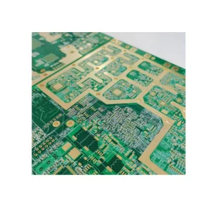
Explore our core product lineup designed for precision computation, heavy industrial applications, and thermal dissipation systems.
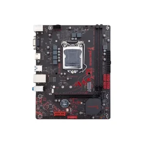
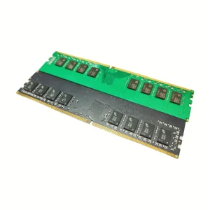
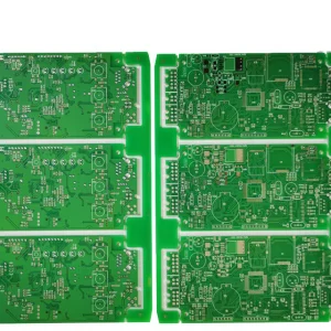
In the contemporary hardware manufacturing landscapes, the term "Thick Copper Circuit Boards" (commonly categorized as Heavy Copper PCBs or Extreme Copper PCBs) refers to printed circuit boards containing finished copper weights greater than 3 oz per square foot (oz/ft²) in either their internal or external layers. Historically, standard PCBs utilized copper foils of 1 oz/ft² (35µm) to 2 oz/ft² (70µm). However, the sweeping global transition toward high-current electrification, green energy storage, and industrial automation has transformed heavy copper fabrication from a niche specialty into an essential industrial vertical.
The global power electronics market demands circuitry that can handle intense current density while simultaneously managing excessive thermal output. High-voltage power distribution blocks, heavy machinery controls, electric vehicle (EV) charging stations, solar panel inverters, and heavy-duty military power supplies require boards capable of carrying up to hundreds of amperes. Thick copper printed circuits provide a structurally sound, highly reliable platform. By integrating thick copper layers into multi-layer configurations, hardware engineers can reduce system complexity, eliminate bulky bus bars, minimize product footprints, and improve the reliability of connection interfaces.
Thick copper circuits function as built-in heat sinks. Heat generated by power-dissipating components is effectively conducted along the heavy trace paths, lowering the junction temperatures of critical semiconductors like MOSFETs and IGBTs.
Heavy copper conductors significantly reduce electrical resistance under high currents. This mitigates I²R power losses, minimizes internal voltage drops, and prevents catastrophic thermal failures on the circuit track.
Heavy copper traces increase the overall physical strength of the substrate. This ensures superior resistance to mechanical stress and thermal fatigue during repetitive thermal expansion cycles.
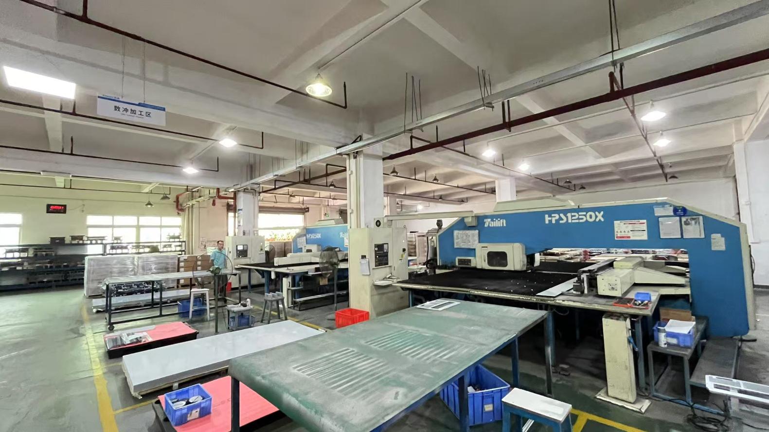
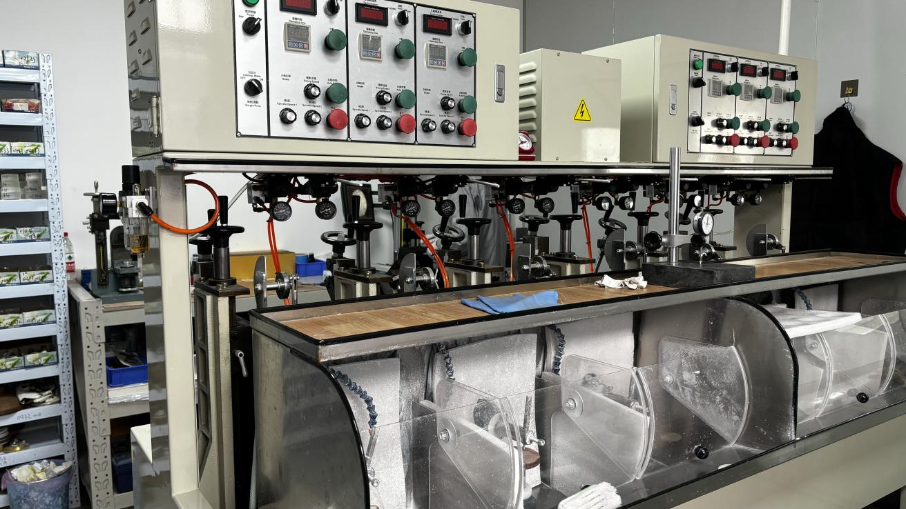
Fabricating heavy copper PCBs requires specialized chemical etching, plating, and lamination processes. As copper thickness increases, standard etching techniques face limitations. Etchant chemistry naturally cuts horizontally under the photoresist mask, causing "undercutting" which distorts the trace cross-section. Advanced Chinese factories utilize specialized differential etching lines and thick-build electroplating equipment to control the etch factor and maintain parallel sidewalls on thick-film structures.
Lamination of thick copper boards also presents challenges. Traditional prepregs struggle to fill the large gaps between thick copper tracks, creating resin voids. To overcome this, advanced manufacturers use specialized high-resin-flow prepregs and high-vacuum multi-stage hot presses. The vacuum lamination process ensures that voids are eliminated and interlayer dielectric strength is maintained.
China's dominance in the global PCB manufacturing sector is driven by supply chain integration, raw material availability, and manufacturing technology. Key advantages include:
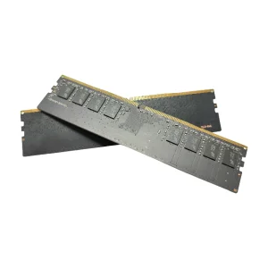
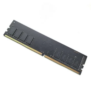
Velmix Technology Co., Ltd. is a professional DDR5 memory manufacturer based in Shenzhen, China, specializing in the research, development, production, and global distribution of high-performance DRAM memory solutions. Since its establishment in 2017, Velmix has been committed to delivering reliable, high-speed memory products for consumer electronics, industrial applications, gaming systems, servers, and embedded computing.
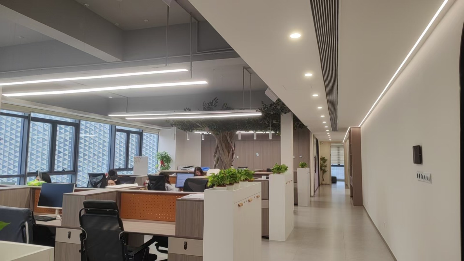
Operating from a modern manufacturing facility covering 368㎡, we combine advanced production technologies with strict quality management to ensure every memory module meets international performance and reliability standards. Our experienced engineering team continuously develops innovative DDR5 memory solutions to meet the evolving demands of AI computing, edge devices, cloud infrastructure, and next-generation computing platforms.
Today, Velmix serves customers in more than 40 countries and regions, offering flexible OEM and ODM manufacturing services for global brands, distributors, system integrators, and industrial equipment manufacturers. By focusing on product consistency, fast delivery, and technical innovation, we have built long-term partnerships across Europe, North America, Southeast Asia, and the Middle East.
| Item | Information |
|---|---|
| Company Name | Velmix Technology Co., Ltd. |
| Established | 2017 |
| Facility Area | 368㎡ |
| Annual Export Revenue | USD 18.6 Million |
| Export Experience | 8 Years |
| Industry Experience | 15 Years |
| Quality Control | 100% Full Inspection Before Shipment |
| Product Inspection Methods | Signal Integrity Test, Burn-in Test, Compatibility Test, Functional Test & Random Sampling |
| QC Staff | 56 Employees |
| Business Type | Manufacturer & Exporter |
| Main Markets | North America, Europe, Southeast Asia, Middle East & South America |
| Supply Chain Partners | 986+ |
| Main Customer Types | Brand Owners, OEM Manufacturers, System Integrators, Distributors & Wholesalers |
| R&D Capability | Independent Product Design, PCB Development & Firmware Optimization |
| Customization Options | OEM, ODM, Private Label, Customized Capacity, Heat Spreader, PCB Color & Packaging |
| New Products Launched Last Year | 138 Models |
| R&D Engineers | 84 Engineers |
Driven by innovation, precision manufacturing, and customer-oriented service, Velmix continues to expand its portfolio of DDR5 memory products while helping global partners build faster, more reliable, and more efficient computing systems. We are dedicated to becoming a trusted long-term supplier of premium memory solutions for customers worldwide.

The mechanical, chemical, and electrical properties of thick copper circuits make them suitable for several key applications. These boards are widely used in fields that require high power transmission, reliability, and thermal management.
Solar photovoltaic inverters and wind turbine power converts require high current throughput. Thick copper substrates handle the current load and withstand temperature swings in outdoor equipment housings.
Electric and hybrid vehicle drivetrains demand heavy-duty boards for battery management systems (BMS), DC-to-DC converters, and motor control units. Heavy copper trace layouts support fast DC charging rates up to 350 kW.
High-power rectifiers, uninterrupted power supplies (UPS), welding systems, and factory automation motor controllers use thick copper boards to manage heavy electrical loads without overheating.
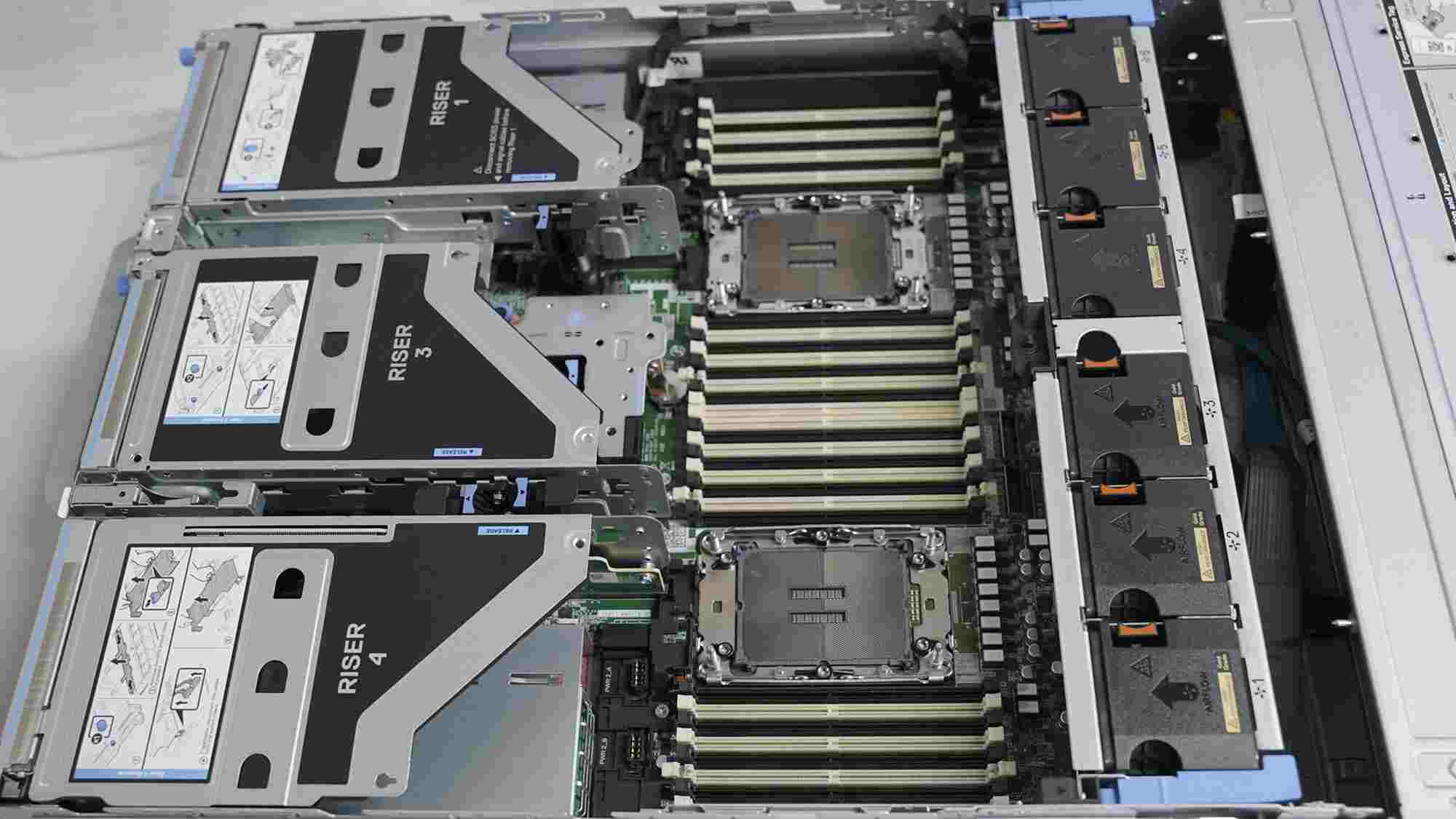
Modern enterprise servers, GPU clusters for AI computing, and cloud systems consume considerable power. Power Distribution Boards (PDBs) and Voltage Regulator Modules (VRMs) in these servers utilize heavy copper PCBs. These multi-layer designs route hundreds of amperes of power at low voltages directly to high-wattage processors and memory interfaces (like DDR5 DRAM systems), maintaining signal integrity and power efficiency.
When sourcing heavy copper PCBs from China, technical specifications should be clearly defined to ensure quality and reliability. Key parameters for the procurement phase include:
A: Standard PCBs typically use copper weights between 0.5 oz and 2 oz. A board is categorized as heavy copper (or thick copper) when it features finished copper weights exceeding 3 oz/ft² (approximately 105µm) on the inner or outer layers.
A: Copper has a high thermal conductivity rating (~385 W/m·K). Thicker copper layers act as heat sinks, spreading localized heat across the board's surface area. This lowers thermal resistance and makes heat dissipation to external cooling assemblies more efficient.
A: Trace spacing must scale with copper thickness to prevent short-circuiting during etching. As a general rule, a 3 oz finished copper layer requires a minimum trace width/spacing of 10 mils (0.25mm), while a 5 oz layer requires 15 mils (0.38mm) or more.
A: High-power systems run at higher operating temperatures. Standard FR4 (Tg 130-140°C) may expand unevenly at these temperatures, causing trace delamination. Specifying high-Tg laminates (Tg ≥ 170°C) helps maintain mechanical stability under high thermal loads.
A: Yes. Modern multi-layer designs use varying copper weights on different layers. For example, outer layers can use thin copper for high-density routing, while inner layers contain thick copper for power distribution.
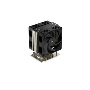
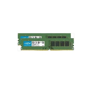
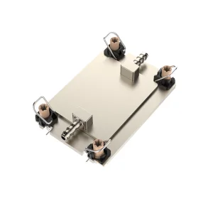
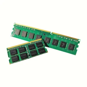
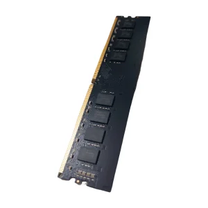
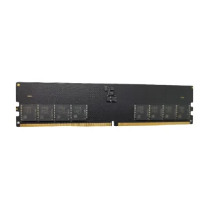
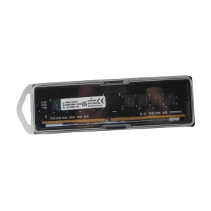
Our comprehensive range of high-current power distribution assemblies, server memories, and thermal accessories.
 Velmix