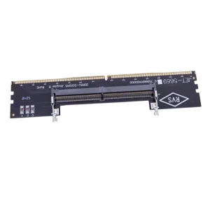
In the rapidly evolving landscape of high-frequency telecommunications, AI-driven server architectures, and high-density packaging, the quality of a PCB prototype defines the line between product innovation and field failure. Printed Circuit Board (PCB) prototyping is no longer merely a preliminary step to check connectivity; it is a critical optimization phase where Signal Integrity (SI), Power Integrity (PI), and Thermal Management are engineered to perfection. As computing modules transition to high-speed standards such as DDR5 and PCIe Gen 5/6, manufacturers must deploy state-of-the-art lithography, impedance control, and substrate selection to meet rigorous signal loss tolerances.
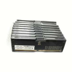
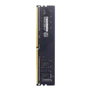
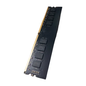
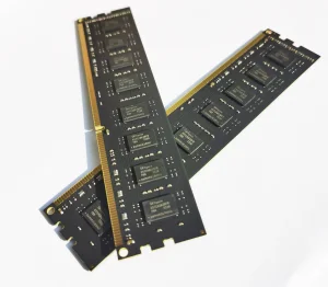
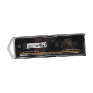
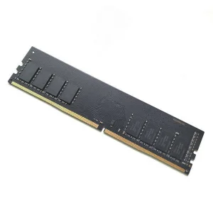
DDR5 memory modules operating up to 6000MHz require routing configurations with sub-picosecond propagation delay tolerances, necessitating advanced HDI (High Density Interconnect) stackups.
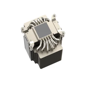
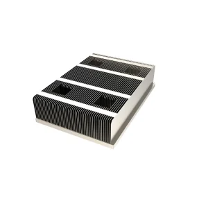
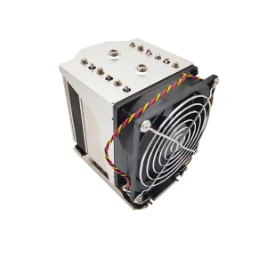
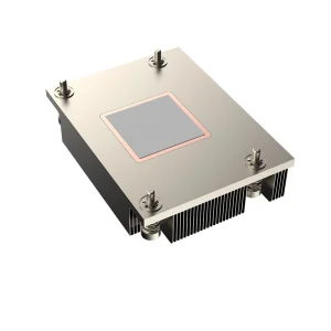
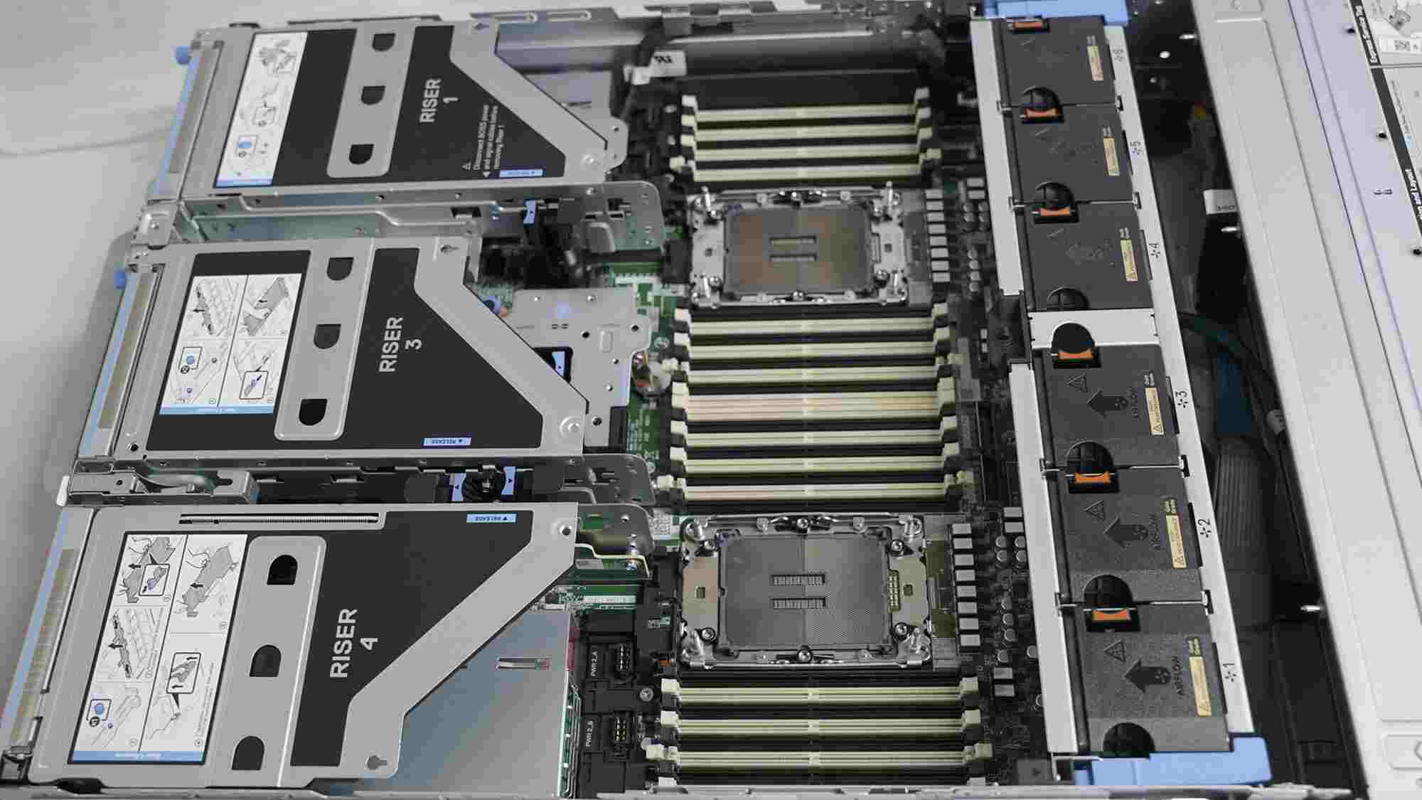
Integrating high-wattage components (e.g., LGA4189/LGA4677 CPUs running up to 400W) demands PCB prototypes featuring localized thick copper backings, embedded thermal vias, or hybrid metal-core substrates.
Transitioning beyond standard FR-4 to low-loss, high-Tg materials like Rogers or Panasonic Megtron 6 to control dissipation factor (Df) and dielectric constant (Dk) at high frequencies.
Velmix Technology Co., Ltd. is a professional DDR5 memory manufacturer based in Shenzhen, China, specializing in the research, development, production, and global distribution of high-performance DRAM memory solutions. Since its establishment in 2017, Velmix has been committed to delivering reliable, high-speed memory products for consumer electronics, industrial applications, gaming systems, servers, and embedded computing.
Operating from a modern manufacturing facility, we combine advanced production technologies with strict quality management to ensure every memory module meets international performance and reliability standards. Our experienced engineering team continuously develops innovative DDR5 memory solutions to meet the evolving demands of AI computing, edge devices, cloud infrastructure, and next-generation computing platforms.
Today, Velmix serves customers in more than 40 countries and regions, offering flexible OEM and ODM manufacturing services for global brands, distributors, system integrators, and industrial equipment manufacturers. By focusing on product consistency, fast delivery, and technical innovation, we have built long-term partnerships across Europe, North America, Southeast Asia, and the Middle East.
| Capability Item | Technical & Operational Details |
|---|---|
| Company Name | Velmix Technology Co., Ltd. |
| Established | 2017 |
| Facility Area | 368㎡ (Dedicated High-Precision Prototyping & Testing Facility) |
| Annual Export Revenue | USD 18.6 Million |
| Export Experience | 8 Years |
| Industry Experience | 15 Years |
| Quality Control | 100% Full Inspection Before Shipment |
| Product Inspection Methods | Signal Integrity Test, Burn-in Test, Compatibility Test, Functional Test & Random Sampling |
| QC Staff | 56 Employees |
| Business Type | Manufacturer & Exporter |
| Main Markets | North America, Europe, Southeast Asia, Middle East & South America |
| Supply Chain Partners | 986+ |
| Main Customer Types | Brand Owners, OEM Manufacturers, System Integrators, Distributors & Wholesalers |
| R&D Capability | Independent Product Design, PCB Development & Firmware Optimization |
| Customization Options | OEM, ODM, Private Label, Customized Capacity, Heat Spreader, PCB Color & Packaging |
| New Products Launched Last Year | 138 Models |
| R&D Engineers | 84 Engineers |
The Chinese manufacturing ecosystem has shifted from a low-cost assembly hub to the global benchmark for Factory 4.0 integration. Shenzhen, serving as the heart of this technological leap, provides unprecedented supply chain resilience. Through localized clusters, components, raw materials, copper-clad laminates (CCL), and packaging are sourced within a 1-hour logistics radius.
For international procurers, this proximity translates directly into agile prototyping timelines. A complex 12-layer HDI PCB prototype that would typically require 3 to 4 weeks in Western facilities can be fabricated, populated (SMT), and tested in China in as little as 3 to 5 days, without compromising on quality or documentation.
Furthermore, our manufacturing incorporates automated optical inspection (AOI), 3D X-Ray laminography (AXI), and in-circuit testing (ICT) directly into the assembly loop. These systems are powered by real-time MES (Manufacturing Execution Systems) software, ensuring full traceabilty of trace width tolerances, copper plating consistency, and reflow profile metrics for every serial-numbered board.
As electronic assemblies shrink and operating frequencies scale toward the millimeter-wave spectrum, the PCB manufacturing roadmap must adapt to several disruptive trends:
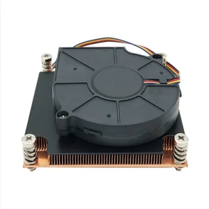
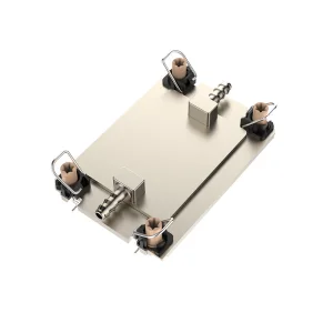
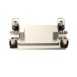
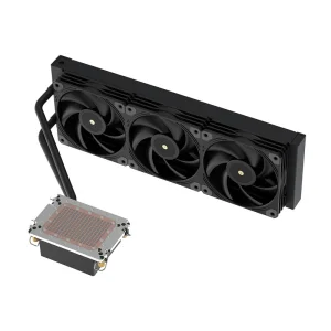
Velmix's forward-looking research focuses on the thermal-electrical optimization of high-speed memories. The integration of copper-based liquid cooling blocks directly with the motherboard, alongside heat dissipating backing plates, ensures that high-power DDR5 DRAM modules maintain peak performance without thermal throttling under continuous workloads.
High-reliability PCB prototyping demands tailor-made workflows depending on the final application vertical. We offer comprehensive engineering adaptations across diverse industries:
Designing multi-layer backplanes up to 32 layers. Support for thick copper planes to deliver stable power to GPU grids, paired with custom water-cooling interfaces for SP5 and LGA4677 chip architectures.
Compliance with Grade 1 automotive thermal standards. Prototyping robust ceramic-filled substrates (MCPCBs) that withstand thermal shocks and high mechanical vibrations in electric vehicle drivetrains.
Polyimide-based PCBs utilizing Class 3 IPC assembly guidelines to guarantee performance under severe radiation, low atmospheric pressures, and extreme G-forces.
Procuring PCB assemblies and prototypes from overseas manufacturers requires managing risks related to timing, fabrication tolerances, and communication transparency. When evaluating an offshore supplier, system integrators and OEMs should prioritize the following verification parameters:
Our operational models are tailored to meet localized environmental, legal, and safety frameworks. By validating every raw material, we guarantee international market viability for all developed assemblies.
Our facility strictly complies with IPC-A-600 and IPC-A-610 Class 2/3 standards. We adhere to green-manufacturing practices through the adoption of halogen-free materials and lead-free surface finishes (such as ENIG - Electroless Nickel Immersion Gold and OSP - Organic Solderability Preservatives), allowing for seamless certification under RoHS, WEEE, and REACH. Additionally, CE and FCC conformance validation guarantees electromagnetic compatibility (EMC) for all integrated system-level assemblies exported to Europe and North America.
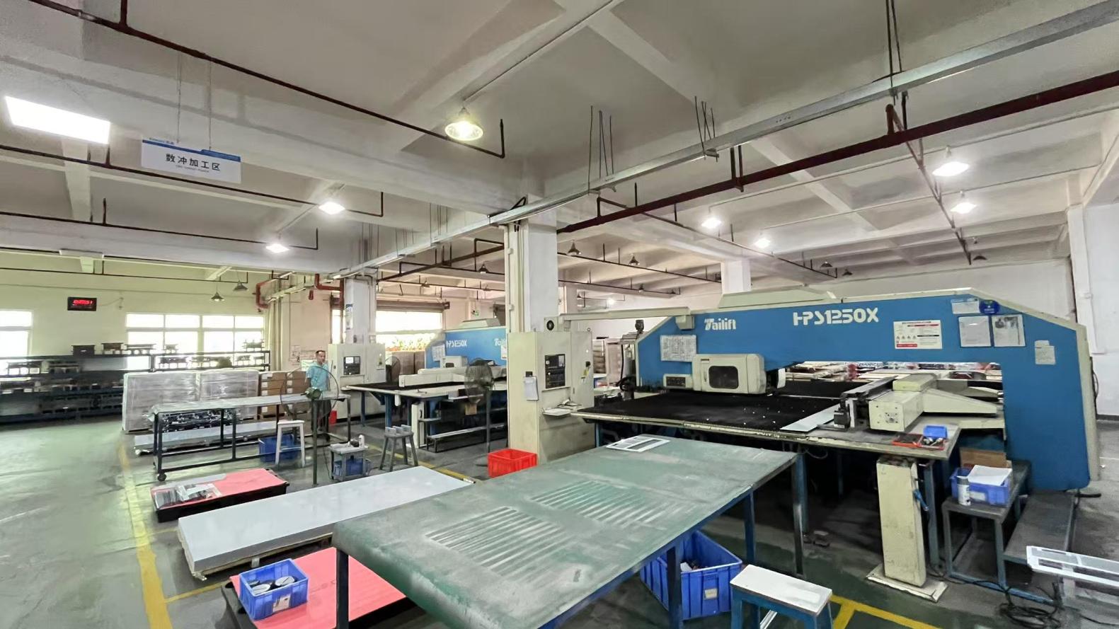
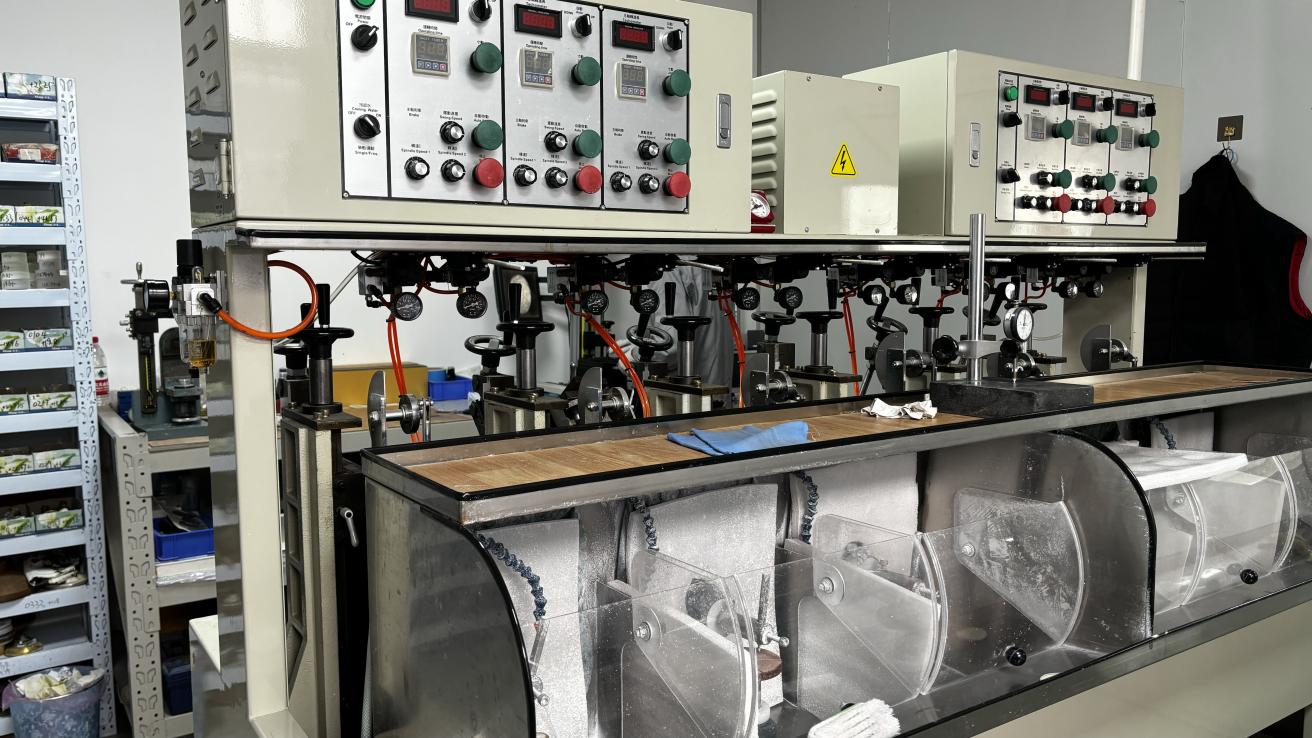
Every production line is structured to maximize high-efficiency throughput, offering cleanrooms for precision SMT assembly, specialized liquid cooling component production, and diagnostic departments checking DRAM modules under temperature-controlled stresses.

 Velmix