Providing precision engineering and rugged thermal architecture designed for stable signal integrity in extreme workloads.
Years of Industry Expertise
R&D Engineers
Full Pre-Shipment Inspection
Countries Served Worldwide
In the rapidly evolving landscape of telecommunications, high-performance computing, and automotive radar networks, High-Frequency Circuit Boards (HF PCBs) have transitioned from specialized components to fundamental hardware building blocks. These circuit boards are engineered to operate at signal frequencies ranging from 500 MHz up to 100 GHz and beyond, where traditional FR-4 materials suffer from catastrophic signal degradation.
At these elevated frequencies, electromagnetic waves travel primarily along the surface of conductors (the skin effect), and dielectric absorption by the board substrate becomes a dominant source of signal loss. Precision impedance control, low loss tangents (Df), and controlled dielectric constants (Dk) are critical to maintaining signal integrity (SI) and power integrity (PI) in multi-gigabit data transmission lines.
The performance of a high-frequency circuit board is fundamentally determined by its raw materials and mechanical layout. Unlike standard multi-layer FR-4 boards, HF boards rely on specialized polymer systems and glass reinforcements to limit thermal dissipation and capacitive coupling.
As a leading supplier in China, we source and process premium raw materials to match exact mechanical and electrical requirements:
Differential signaling channels require strict trace width and spacing tolerance of within ±5% to prevent signal reflection at Gigabit speeds.
By leveraging ultra-low dissipation factor (Df) laminates, signal attenuation is minimized, maintaining eye-diagram opening margins.
Integrating direct thermal vias and thick copper backing prevents thermal degradation of surface-mounted microprocessors and RF power amplifiers.
Global procurement teams targeting China wholesale channels for high-frequency PCBs face multifaceted compliance, quality control, and shipping requirements. In recent years, purchasing strategies have shifted from raw unit-cost minimization toward long-term component lifecycle reliability and supply-chain transparency.
Key requirements for international procurement include:
Velmix Technology Co., Ltd. is a professional DDR5 memory manufacturer based in Shenzhen, China, specializing in the research, development, production, and global distribution of high-performance DRAM memory solutions. Since its establishment in 2017, Velmix has been committed to delivering reliable, high-speed memory products for consumer electronics, industrial applications, gaming systems, servers, and embedded computing.
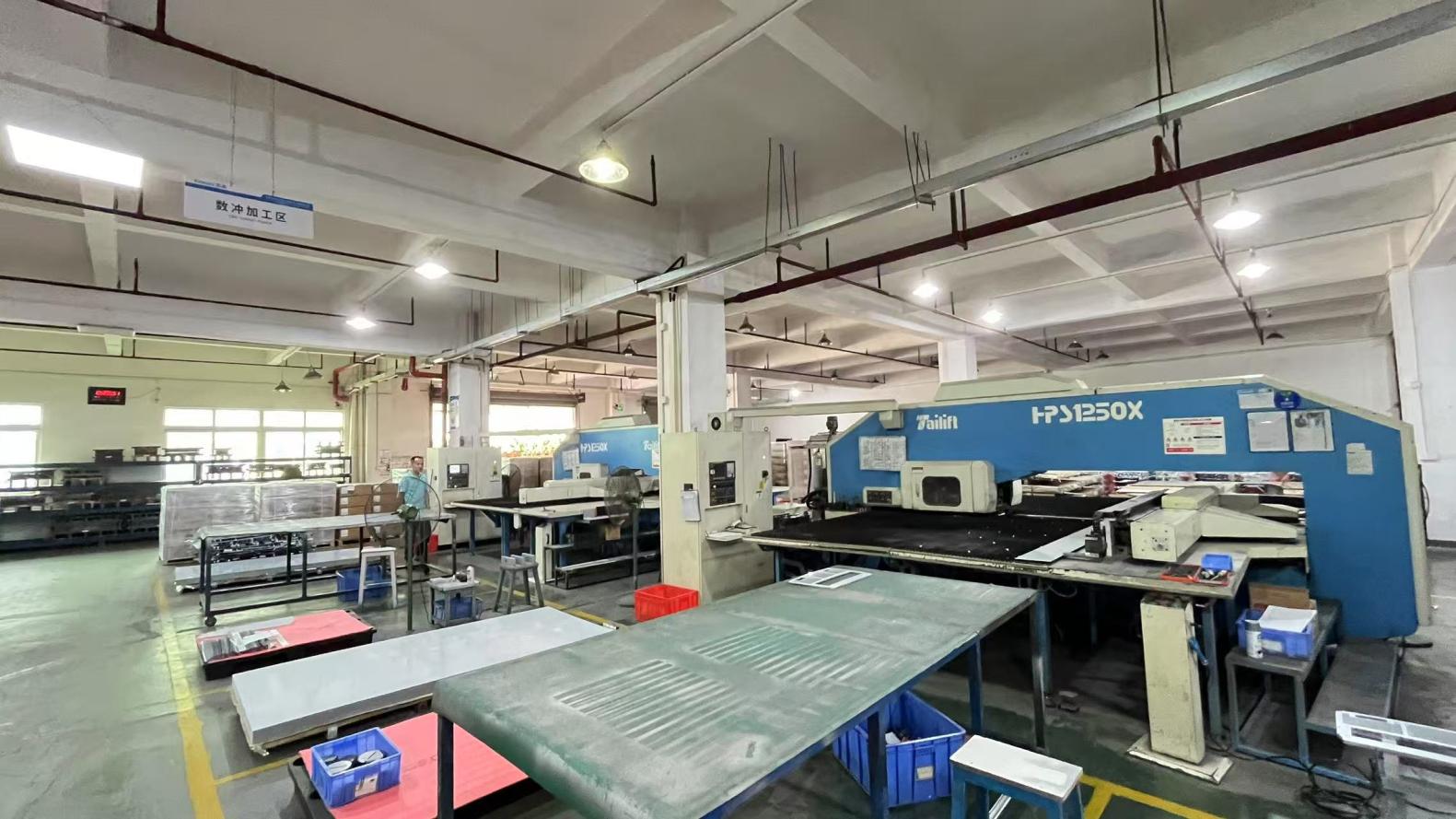
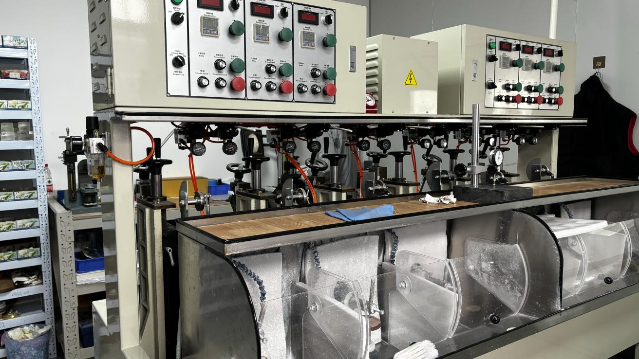
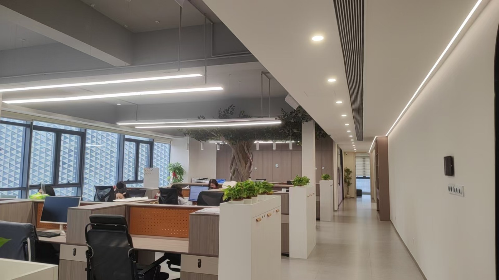
Operating from a modern manufacturing facility covering 368㎡, we combine advanced production technologies with strict quality management to ensure every memory module meets international performance and reliability standards. Our experienced engineering team continuously develops innovative DDR5 memory solutions to meet the evolving demands of AI computing, edge devices, cloud infrastructure, and next-generation computing platforms.
Today, Velmix serves customers in more than 40 countries and regions, offering flexible OEM and ODM manufacturing services for global brands, distributors, system integrators, and industrial equipment manufacturers. By focusing on product consistency, fast delivery, and technical innovation, we have built long-term partnerships across Europe, North America, Southeast Asia, and the Middle East.
| Item | Information |
|---|---|
| Company Name | Velmix Technology Co., Ltd. |
| Established | 2017 |
| Facility Area | 368㎡ |
| Annual Export Revenue | USD 18.6 Million |
| Export Experience | 8 Years |
| Industry Experience | 15 Years |
| Quality Control | 100% Full Inspection Before Shipment |
| Product Inspection Methods | Signal Integrity Test, Burn-in Test, Compatibility Test, Functional Test & Random Sampling |
| QC Staff | 56 Employees |
| Business Type | Manufacturer & Exporter |
| Main Markets | North America, Europe, Southeast Asia, Middle East & South America |
| Supply Chain Partners | 986+ |
| Main Customer Types | Brand Owners, OEM Manufacturers, System Integrators, Distributors & Wholesalers |
| R&D Capability | Independent Product Design, PCB Development & Firmware Optimization |
| Customization Options | OEM, ODM, Private Label, Customized Capacity, Heat Spreader, PCB Color & Packaging |
| New Products Launched Last Year | 138 Models |
| R&D Engineers | 84 Engineers |
Driven by innovation, precision manufacturing, and customer-oriented service, Velmix continues to expand its portfolio of DDR5 memory products while helping global partners build faster, more reliable, and more efficient computing systems. We are dedicated to becoming a trusted long-term supplier of premium memory solutions for customers worldwide.

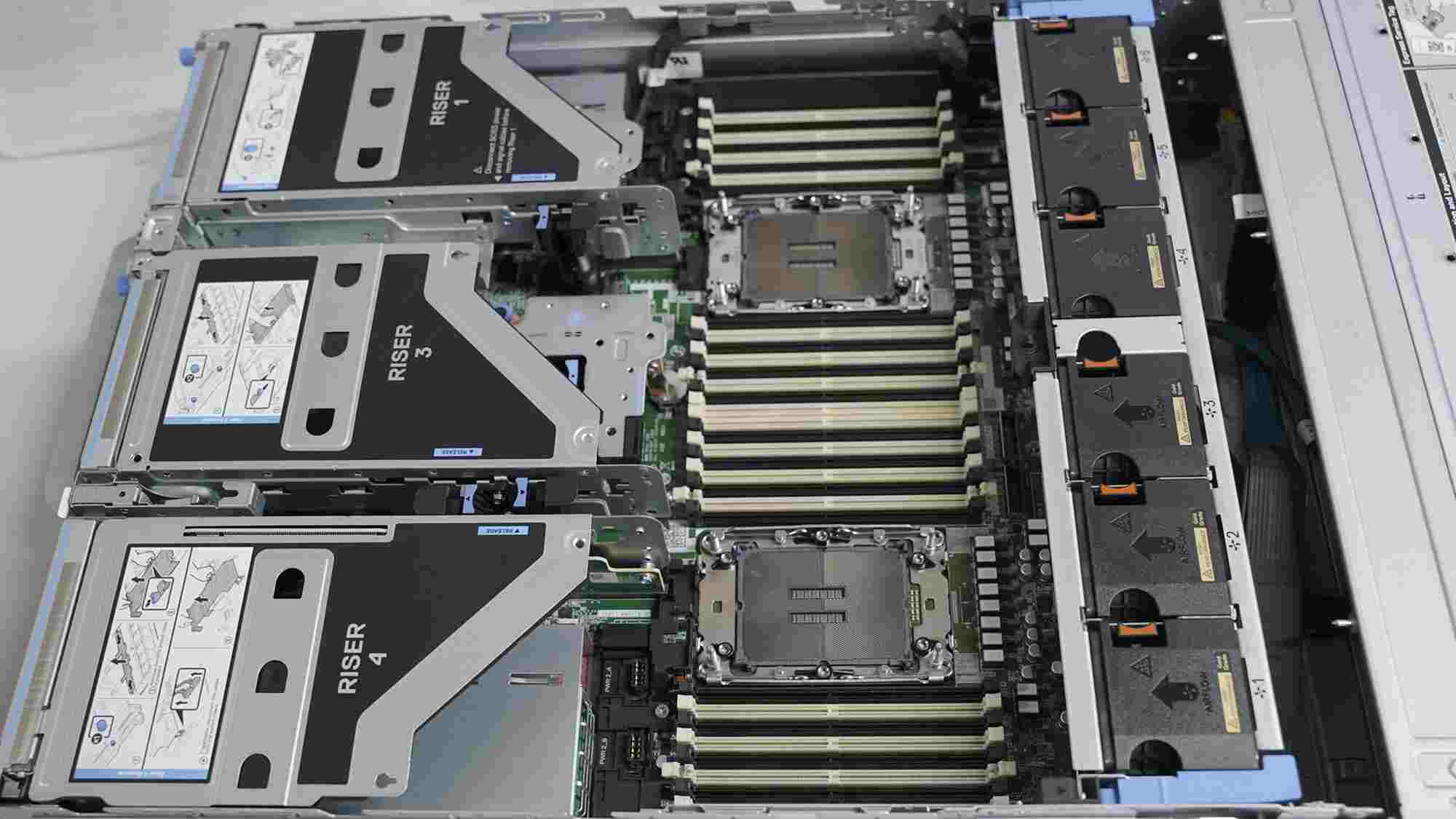
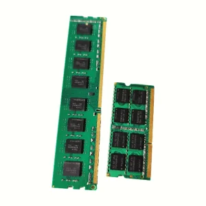
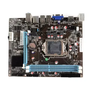
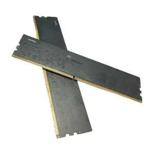
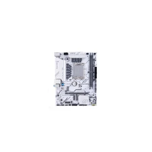
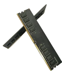
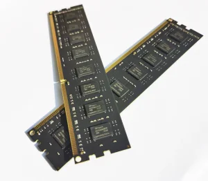
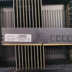
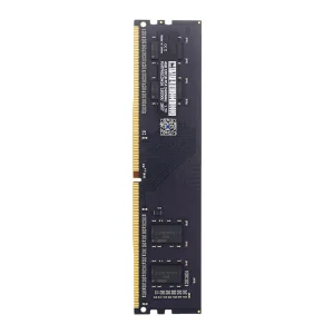
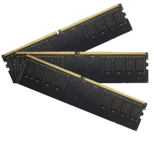
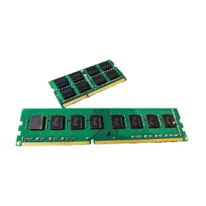
The structural synergy between high-frequency substrates and system components cannot be overstated. When engineering memory modules (such as DDR4 or DDR5) or processor motherboards (such as the H610 and H61 lines), transmission line geometry must account for pin-out configurations and cooling topologies.
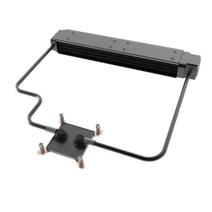
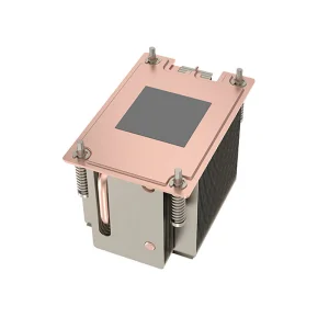
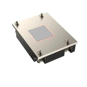
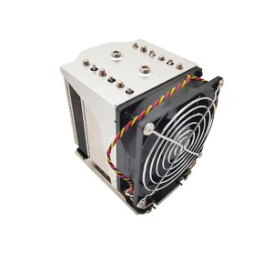
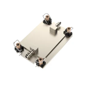
For instance, high-speed RAM layouts (running up to 3200MHz and beyond) require exact matched trace lengths to minimize phase deskew. Meanwhile, server boards supporting high-power CPUs require deep thermal dissipation channels. Liquid cooling radiators, copper heatsinks, and optimized passive cooling mechanisms must line up with the board's internal routing layers to prevent localized hot spots that alter the board's dielectric constant.
Our commitment to reliability is demonstrated through testing protocols that ensure signal stability across extreme environments:
As industry standards transition toward PCIe Gen 6/7, 6G communications, and ultra-dense computing networks, High-Frequency PCBs must adapt to increasingly demanding physical constraints. Key technological trends driving our future R&D efforts include:
Get quick answers regarding technical specifications, design assistance, custom manufacturing, and ordering processes.
For applications exceeding 10 GHz, we recommend PTFE-based substrates or hydrocarbon ceramics with a dissipation factor (Df) below 0.003. Popular materials include Rogers 4350B, Rogers 3003, and Megtron 6, depending on mechanical rigidity requirements.
We employ continuous online tracking coupled with automated wet etching controls. We run regular coupon testing on every manufacturing panel using TDR (Time Domain Reflectometry) to guarantee that impedance tolerances remain within ±5% to ±7% of target designs.
Standard prototype lead times range from 5 to 7 working days, depending on material availability and stack-up complexity. For complex multi-layer designs or hybrid laminations, the cycle can extend up to 10 to 12 working days.
Yes, we specialize in cost-effective hybrid board construction. By placing low-loss Rogers or Megtron layers on the outer routing channels and utilizing standard FR-4 layers for internal power or signal pathways, we optimize cost and performance.
Yes, all wholesale shipments include testing and validation documentation, including TDR impedance reports, cross-section micrographs, solderability certifications, and RoHS compliance documentation.
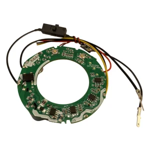
High-stability component boards, active server cooling units, and high-performance memory modules.
 Velmix