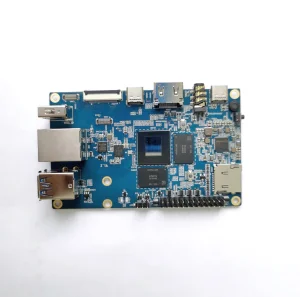
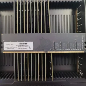
Explore our engineering capabilities in multi-layer system architecture, memory integration, and high-frequency PCBA solutions.
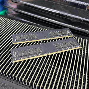
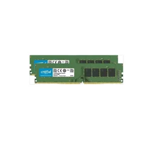
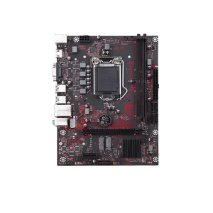
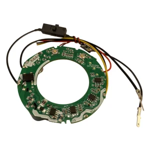
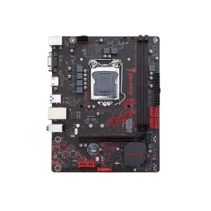
Modern electrical engineering demands higher data transfer rates, reduced electromagnetic interference (EMI), and shrinking physical footprints. Multilayer Printed Circuit Boards (PCBs) represent the solution to this multi-dimensional constraint space. By sandwiching multiple conductive copper trace pathways between insulating dielectric prepreg and core materials, multilayer PCBs enable high-density routing options that single- or double-sided boards cannot sustain.
At Velmix Technology Co., Ltd., we produce multilayer PCBs engineered with extreme precision, ranging from 4 up to 32 layers. Achieving reliable impedance control at high frequencies (exceeding 28 GHz) requires highly specific layer assignment strategies, controlled dielectric thickness, and precise trace geometries. Our process uses controlled impedance modeling (using advanced Polar Instruments software) to align microstrip, stripline, and differential pair impedance target tolerances within ±5%.
Our material supply chain ensures access to high-temperature FR-4 (Tg > 170°C), halogen-free substrates, and low-loss High-Frequency laminates (such as Rogers, Isola, and Shengyi). These materials exhibit ultra-low dissipation factor ($D_f$) and stable dielectric constant ($D_k$) variations, preventing high-speed signal attenuation and phase mismatch across large arrays of differential channels.
From deep-learning hardware modules to mission-critical automotive safety arrays, see how our multi-layered circuit technologies empower global industries.
AI processing models require massive bandwidth. Our PCB stack-ups are optimized for DDR5, GDDR6, and PCIe Gen 5 configurations, implementing micro-vias, buried vias, and back-drilling to eliminate stub reflections in complex motherboards.
As board densities increase, thermal accumulation degrades reliability. We design customized multilayer PCBs with heavy copper layers (up to 6 oz), metal-backed cores, and copper-filled thermal vias to conduct heat away from processors.
High-Density Interconnect (HDI) structures are essential for packaging microprocessors and fine-pitch BGAs. We build staggered, stacked, and copper-plated vias-in-pad (VIPPO) to maintain circuit paths within trace pitches below 3 mils.
Utilizing high-performance ceramic and PTFE composite laminates, we support sub-6GHz and millimeter-wave RF PCB requirements. These PCBs provide the precision routing needed for ADAS sensor boards and optical network gear.
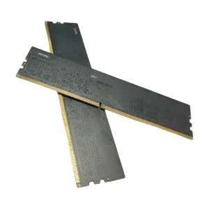
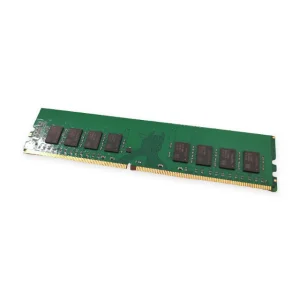
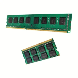
Established in 2017 in Shenzhen, China, Velmix has become a key manufacturer of high-performance DRAM memory, motherboard architectures, and customized PCBA solutions.
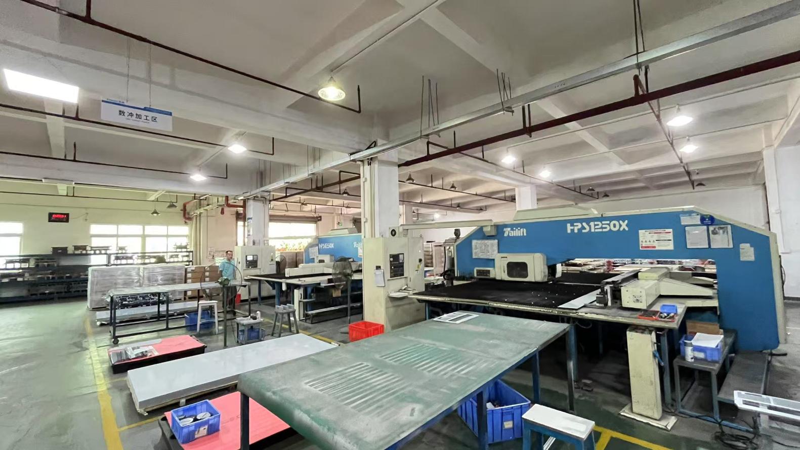
Operating a modern facility with advanced SMT mounting and multi-layer PCB inspection systems, Velmix combines state-of-the-art production with strict quality management to ensure every motherboard, memory module, and custom PCBA meets international standards.
Serving customers in more than 40 countries, our engineering team works with brand owners, distributors, system integrators, and industrial partners globally, providing customized capacity design, layout optimization, thermal design, and firmware adjustments.

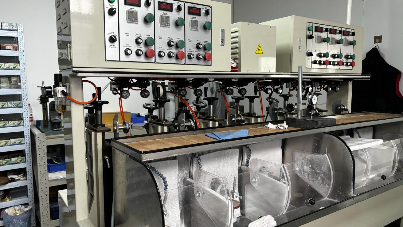
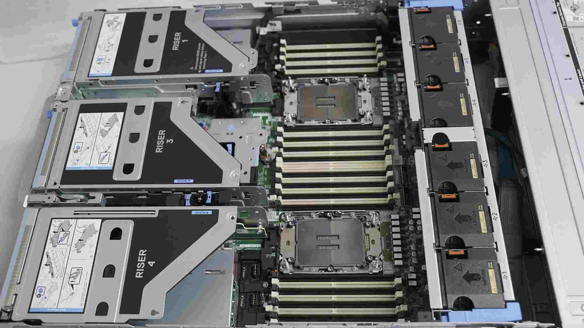
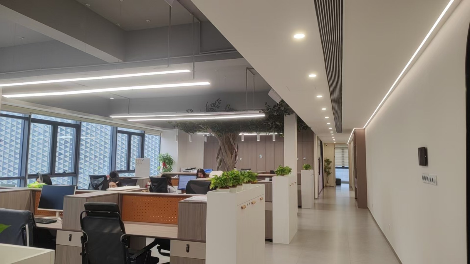
A closer look at our organizational capability, equipment parameters, quality protocols, and customization options.
| Performance & Operation Parameters | Technical Verification / Details |
|---|---|
| Company Name | Velmix Technology Co., Ltd. |
| Established | 2017 |
| Facility Area | 368㎡ |
| Annual Export Revenue | USD 18.6 Million |
| Export Experience | 8 Years |
| Industry Experience | 15 Years |
| Quality Control | 100% Full Inspection Before Shipment |
| Product Inspection Methods | Signal Integrity Test, Burn-in Test, Compatibility Test, Functional Test & Random Sampling |
| QC Staff | 56 Employees |
| Business Type | Manufacturer & Exporter |
| Main Markets | North America, Europe, Southeast Asia, Middle East & South America |
| Supply Chain Partners | 986+ |
| Main Customer Types | Brand Owners, OEM Manufacturers, System Integrators, Distributors & Wholesalers |
| R&D Capability | Independent Product Design, PCB Development & Firmware Optimization |
| Customization Options | OEM, ODM, Private Label, Customized Capacity, Heat Spreader, PCB Color & Packaging |
| New Products Launched Last Year | 138 Models |
| R&D Engineers | 84 Engineers |
Our quality control protocol is structured to verify all electrical trace parameters across extreme environment limits. We inspect raw base copper laminates for void defects, micro-cracks, and grain boundaries using Automated Optical Inspection (AOI) and X-ray imaging before laminating the stack-up layers together.
During via metallization, we implement dry-film lamination and precise copper electroplating to ensure via walls are evenly coated. A key cause of high-frequency signal degradation is non-uniform plating inside blind and buried vias, which causes impedance mismatches and reflection noise. We monitor copper thickness in real-time, aiming for a minimum of 20 microns on all internal via walls.
To verify performance under environmental stress, every production batch undergoes thermal cycling test chambers, lasting from -40°C to 125°C. This ensures the copper trace adhesion and the glass-reinforced epoxy composites match perfectly in thermal expansion coefficient (CTE), preventing delamination over long-term operation.

We manufacture multilayer boards in line with international electronic standards, ensuring safety, reliability, and regulatory compliance for our global partners.
Our manufacturing and SMT assembly lines are ISO 9001 certified. We maintain detailed documentation, step-by-step process monitoring, and tracing systems from raw materials to final shipments.
All multilayer materials we use are UL-listed. We verify self-extinguishing properties (94V-0) under strict vertical burn conditions, protecting computing equipment from heat issues.
We support lead-free assembly processes. Our surface finishes (including ENIG, OSP, and lead-free HASL) comply with RoHS and REACH regulations, meeting environmental rules for European and North American markets.
As computing requirements trend toward higher speeds, our technology continues to develop to support next-generation system demands.
Developing stack-ups with cores down to 1.5 mils to reduce overall board thickness. This allows for higher routing density in mobile devices and advanced consumer electronics.
Integrating resistors and capacitors directly into inner layers of the PCB stack-up. This frees up surface space, reduces parasitic inductance, and improves high-frequency signal integrity.
Researching hybrid copper-optical circuit designs. These configurations combine standard electrical routing with fiber optical paths to support speeds beyond 112 Gbps PAM4 for next-generation telecommunications infrastructure.
A compilation of common questions about multilayer PCBs, stack-up design, manufacturing limits, and ordering processes.
Multilayer PCB costs depend on several key factors: layer count (higher count requires more lamination and material steps), material type (specialized materials like Rogers or High-Tg FR-4 cost more than standard FR-4), trace spacing parameters, surface finish options (ENIG and ENEPIG cost more than HASL), and the configuration of micro-vias or blind/buried vias, which require extra drilling and plating cycles.
We verify controlled impedance by including a test coupon on the edge of each production panel. This coupon mimics the actual signal trace routing parameters of the board. We measure this using Time Domain Reflectometry (TDR) testing to confirm the impedance values fall within the target limits (typically ±10% or ±5% for critical high-speed circuits) before final routing.
Layer symmetry helps prevent board warping during lamination and lead-free soldering cycles. When copper thickness, dielectric thickness, and prepreg material types are symmetric around the center layer of the board, thermal expansion stresses are distributed evenly, helping the board remain flat during high-temperature SMT assembly processes.
Blind vias connect an outer layer to at least one inner layer without going through the entire board. Buried vias connect two or more inner layers together and are not visible from the outside. Micro-vias are small laser-drilled vias (typically under 6 mils in diameter) used in HDI designs, often spanning a single layer, which helps save routing space.
We offer end-to-end design and manufacturing support. Our team of 84 engineers helps partners optimize PCB layouts for manufacturability (DFM), match appropriate materials, manage thermal dissipation, adjust firmware, and perform 100% inspection before shipment to ensure high reliability across consumer, industrial, and server applications.
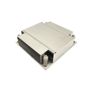
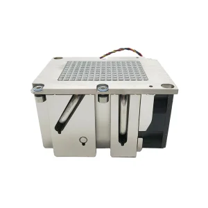
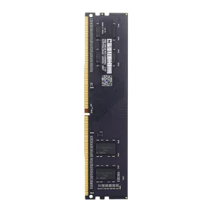
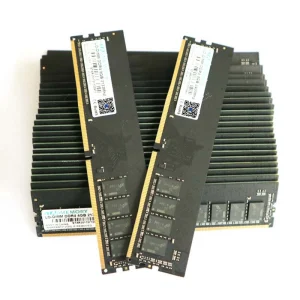
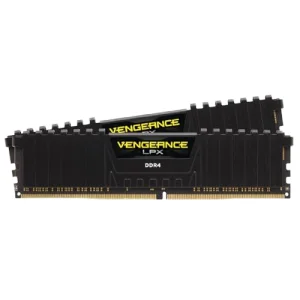
Explore our selection of industrial heatsinks, server radiators, development boards, and specialized memory hardware.
 Velmix