How RAM chips are made in China begins with a silicon wafer, not a finished chip. In cleanrooms, manufacturers deposit thin films, print circuit patterns with photolithography, etch selected layers, and add materials that form transistors and connections. DRAM cells also need tiny capacitors to store electrical charges. The wafer then undergoes electrical testing before it is cut into individual dies and packaged. Small defects matter. One particle can spoil a microscopic pattern.
SEMI’s 2024 World Fab Forecast projected about $50 billion in semiconductor equipment spending in China that year. This figure signals substantial manufacturing investment, but it does not measure Chinese DRAM output alone. That distinction matters: equipment spending, wafer capacity, and successful memory-chip production are not interchangeable. Chris Mack, a semiconductor lithography expert, describes the patterning step as “transferring a pattern from a mask to a wafer.” His explanation captures one stage, not the entire manufacturing chain.
This outline will trace the process from wafer preparation to packaged RAM, while noting where Chinese manufacturers fit into a complex global supply network. Readers will encounter cleanroom tools, repeated deposition and etching cycles, and rigorous testing. The steps sound orderly. Real production is less tidy: yields vary, equipment needs calibration, and public data rarely reveal every company’s process details. That uncertainty deserves attention, rather than a neat but unsupported claim about who makes every chip.
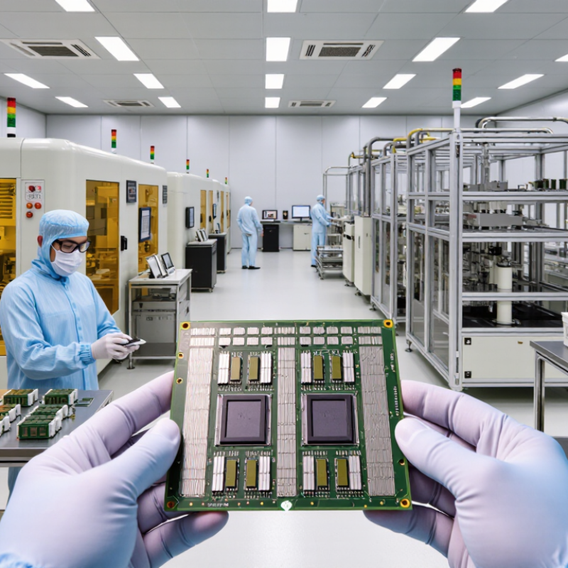
An 8-Gb DRAM device stores 8 billion bits, or 1 GB of raw capacity. That figure does not define the whole product: package design, interface, power limits, and intended use shape the specification. For China-based development teams, planning starts with a clear target, such as mobile memory or a computer module. The design must balance cell-array efficiency with sensing, refresh, and test requirements. At the process level, teams map each design choice to wafer steps, including lithography, etching, and capacitor formation. Yield is unforgiving. Small defects can affect many cells.
Planning also means setting measurable checks for retention, operating voltage, and performance across temperature ranges. A process window that looks stable in a model may behave differently on a production line. The plan needs revision. WSTS’s Autumn 2024 forecast put global memory sales at $165.3 billion for 2024, up 81% year over year. That is a global market estimate, not a China-specific DRAM forecast. It does, however, underline why capacity and product timing matter. Engineers should validate assumptions with wafer data, not market optimism alone. On an 8-Gb-class program, even a modest mismatch between design targets and process capability can erode usable output.
DRAM production starts with a 300 mm silicon wafer: a flat, highly polished disk that provides the foundation for countless memory cells. Its diameter is not just a factory convention. Compared with a 200 mm wafer, it offers 2.25 times the surface area, before edge losses and chip layout are considered. More usable area can mean more dies per wafer. The starting surface matters.
A wafer’s quality is established well before memory patterns are formed. Crystal growth, slicing, polishing, and cleaning must leave a surface with tightly controlled thickness and very few defects. Even tiny particles can interrupt later patterning steps. Clean does not mean perfect. Process engineers still need to detect and manage imperfections across the wafer. That challenge is easy to underestimate.
The scale of this substrate is reflected in industry capacity forecasts. SEMI’s 300mm Fab Outlook projected global 300 mm fab capacity would reach about 9.6 million wafer starts per month by 2026. This figure covers multiple semiconductor uses, not DRAM alone. In Chinese production lines, as elsewhere, the wafer is the common starting platform; the eventual memory design depends on many later process steps. Diameter sets the canvas, but it does not guarantee yield.
At a DRAM fabrication plant in China, each memory bit is built around a 1T1C cell: one transistor and one capacitor. Patterning turns a circuit design into tiny physical features on a silicon wafer. Photolithography transfers selected shapes, while etching and deposition form and refine the layers. A word line controls the transistor gate. A bit line carries signals to and from the cell. The layout must fit billions of repeated structures into a small area. That repetition leaves little room for alignment errors.
The capacitor stores charge as a very small electrical signal. In dense DRAM, its structure often extends vertically, helping provide useful capacitance without taking much surface area. Insulating dielectric layers separate its conductive surfaces. When a word line activates the transistor, the cell connects to a bit line for reading or writing. Simple on paper. Difficult in practice. Tiny shifts in line width, film thickness, or overlay can change cell behavior across a wafer. Process engineers inspect patterns and electrical test results, then adjust manufacturing steps to keep variation under control. Still, a clean measurement does not explain every defect; that gap is a real part of process development.
Before an 8-Gb memory die is separated from its wafer, probe cards touch tiny metal pads and connect each die to automated test equipment. Test patterns exercise memory cells and detect faults such as stuck bits or unwanted interactions. The tester does not simply read eight billion bits one by one; carefully designed patterns expose many defects efficiently. Tiny defects matter.
Test results map good and failing locations across the wafer. Some repairable memory faults can be routed around using redundant rows or columns. After probing, a precision saw separates the wafer into individual dies. Each cut leaves a narrow kerf, and dust or edge chipping can damage otherwise usable silicon.
SEMI’s 2024 silicon-wafer shipment report recorded 12,266 million square inches shipped worldwide, 2.7% below 2023. That figure describes industry scale, not memory-chip yield—a useful distinction when reading manufacturing claims.
Tips: Look for probe-test coverage, repair handling, and post-dicing inspection in process descriptions. A high test pass rate alone does not reveal every source of later failure. And measurement is not perfect.
In China, DRAM packaging may follow a chain of precise steps: wafer inspection, die cutting, attachment to a package substrate, electrical connection, and protective molding. The finished package is then checked for defects before it reaches module assembly. Exact equipment and process details vary between factories, so one production line cannot represent every plant.
For DDR5, VDD is a nominal 1.1 V supply for the memory core. It is a carefully controlled operating target, not a promise that every measurement will read exactly 1.100 V. Engineers check voltage stability, current behavior, and signal quality under changing workloads and temperatures. Small margins matter. A test system may record rail behavior while cycling data patterns, because a chip that works briefly at room temperature may fail after extended use. Module-level power management also needs validation; the memory package alone does not tell the whole story.
Packaging checks can include visual inspection, continuity tests, and functional testing across specified conditions. Technicians may compare results from multiple samples and investigate unusual readings before approving a batch. Not just voltage. I would be cautious about treating a single pass result as proof of long-term reliability; test coverage and traceable records matter too. Even a clean package can reveal weak performance only under a specific combination of heat, load, and timing.
| Stage or Parameter | Process or Typical Data | Purpose and Validation |
|---|---|---|
| Wafer preparation | Completed DRAM circuits are fabricated on a silicon wafer, then electrically probed before individual dies are separated. | Wafer probing identifies dies that fail initial electrical checks before packaging. |
| Die separation and assembly | The wafer is cut into individual dies. Dies are attached to package substrates or lead frames and connected using an assembly method suited to the package design. | Assembly inspection checks die placement, connections, and package integrity. Specific methods vary by product. |
| Encapsulation and marking | The assembled die is protected within a package; the package is then finished and marked for identification and traceability. | Visual and mechanical inspections look for defects such as package damage, contamination, or incorrect marking. |
| DDR5 VDD supply | DDR5 DRAM uses a nominal VDD supply of 1.1 V. The permitted operating range and test limits depend on the applicable specification and device conditions. | Electrical tests verify operation at specified supply conditions. VDD is the DRAM core supply; it should not be confused with every other rail in a system. |
| Other DDR5 supply rails | DDR5 designs also use other supply rails. For example, VPP is nominally 1.8 V; rail requirements depend on the device and implementation. | Each required rail is checked against the relevant device and system specifications rather than assumed to share the VDD value. |
| Module power management | On many DDR5 memory modules, a power-management integrated circuit on the module regulates or distributes operating voltages from the input supply. | Module-level checks confirm that power delivery is stable and that the memory operates correctly under specified conditions. |
| Functional and timing tests | Test patterns exercise memory locations, read and write operations, and timing behavior across supported operating conditions. | These tests detect functional faults and help verify that the device meets its specified timing limits. |
| Temperature and reliability screening | Devices may be tested or screened at defined temperature and stress conditions according to the product qualification plan. | Results help assess operation and reliability within the intended rated conditions; exact procedures vary by product. |
| Final sorting and shipment | Passing devices are classified according to tested characteristics and packaged for handling and shipment. | Final records maintain traceability and confirm that shipped parts meet their specified acceptance criteria. |
Each bit uses one transistor and one capacitor. The transistor connects the cell to a bit line when its word line activates.
It holds a tiny electrical charge. Conductive surfaces and an insulating layer help store that signal in a compact space.
Billions of repeated structures leave little room for shifts. Small changes in line width or film thickness can affect cell behavior.
Probe cards touch small metal pads on the wafer. Automated tests use patterns to find stuck bits and unwanted cell interactions.
Some faults can be bypassed with spare rows or columns. Not every defect is repairable, and test results do not show everything.
A precision saw separates each die, leaving a narrow cut. Dust or chipped edges can damage usable silicon. Small details matter.
A die is attached to a package substrate, electrically connected, and covered with protective molding. Factories may use different equipment and steps.
It is the nominal core supply target, not a guarantee of an exact reading. Engineers check voltage stability under changing workloads and temperatures.
No. Testing multiple samples across heat, load, and timing can reveal weaknesses. A single pass still leaves questions.
How RAM chips are made begins with careful design and process planning for an 8-Gb-class memory product. Production starts on a polished 300 mm silicon wafer, which provides the foundation for many chips. Repeated patterning and fabrication steps create dense memory arrays, with each bit built around a 1T1C cell: one transistor controls access to one capacitor that stores the bit’s charge.
Once the wafer is complete, electrical probing checks the dies and identifies defects before the wafer is diced into individual chips. Each 8-Gb die must reliably store and retrieve billions of bits. The selected dies are packaged and then tested under operating conditions, including validation for DDR5 use with a 1.1 V VDD supply. These stages turn microscopic structures on a wafer into memory chips ready for integration into electronic systems.

Velmix